Silicon chip prealignment device and silicon chip prealignment method

A pre-aligned, silicon wafer technology, applied in the field of lithography, which can solve the problems of not considering the influence of the measurement accuracy of the wafer, the influence of the measurement value of the edge of the wafer, the influence of the centering and orientation accuracy of the wafer, etc.

Active Publication Date: 2012-04-04
SHANGHAI MICRO ELECTRONICS EQUIP (GRP) CO LTD
View PDF5 Cites 20 Cited by
  • Summary
  • Abstract
  • Description
  • Claims
  • Application Information

AI Technical Summary

Problems solved by technology

[0003] The current common pre-alignment method is to measure the edge position of the silicon wafer through the sensor, and the silicon wafer can be rotated once to obtain all the edge positions of the silicon wafer, and the center and direction of the silicon wafer can be obtained by fitting, but due to silicon During the rotation of the wafer, it is inevitable to vibrate in the vertical direction. This vibration will affect the measured value of the edge of the silicon w...

Method used


Image

  • Silicon chip prealignment device and silicon chip prealignment method
  • Silicon chip prealignment device and silicon chip prealignment method
  • Silicon chip prealignment device and silicon chip prealignment method

Examples


Embodiment Construction

[0029] In the following, preferred embodiments according to the present invention will be described in detail with reference to the accompanying drawings. For the convenience of describing and highlighting the present invention, relevant components existing in the prior art are omitted from the drawings, and the description of these known components will be omitted.

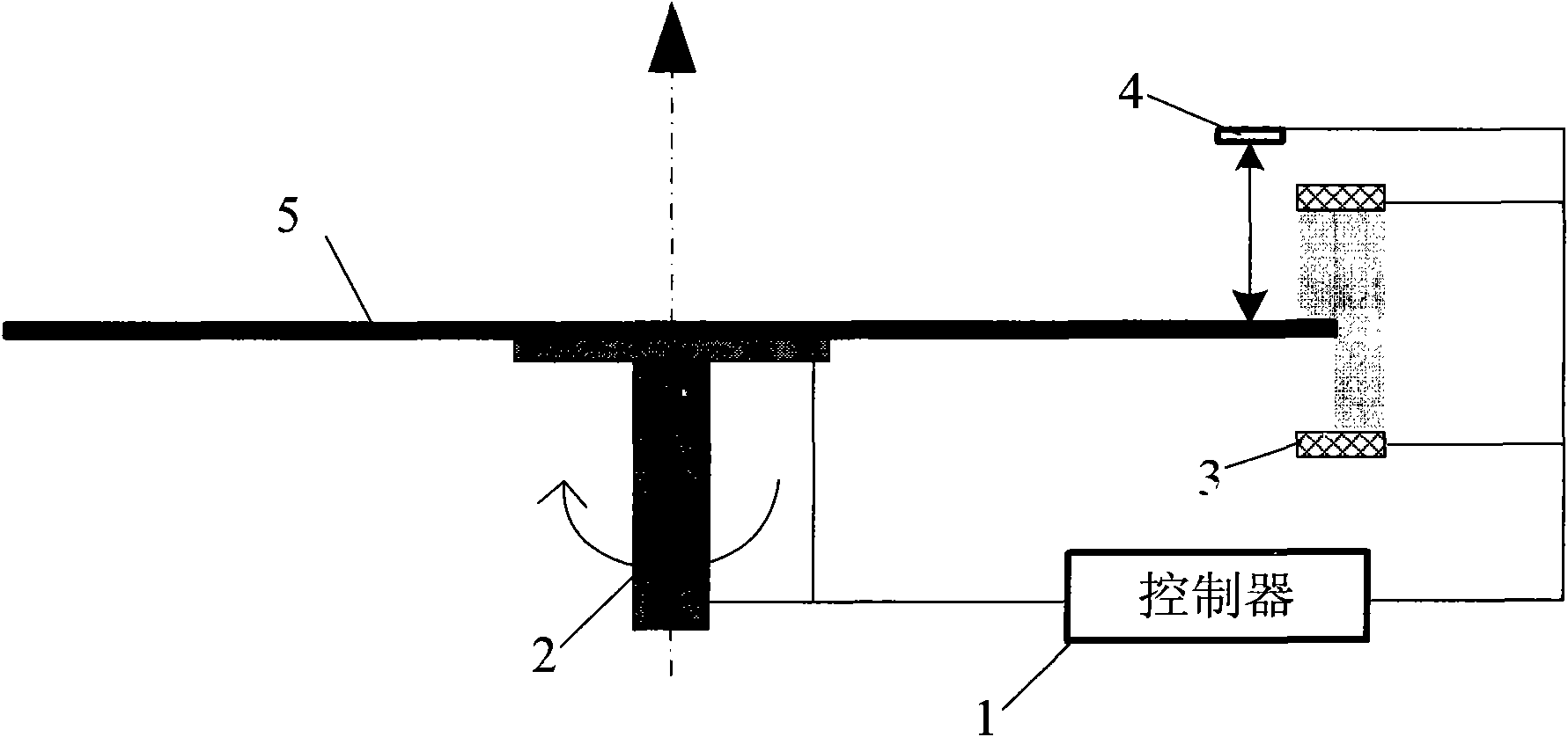
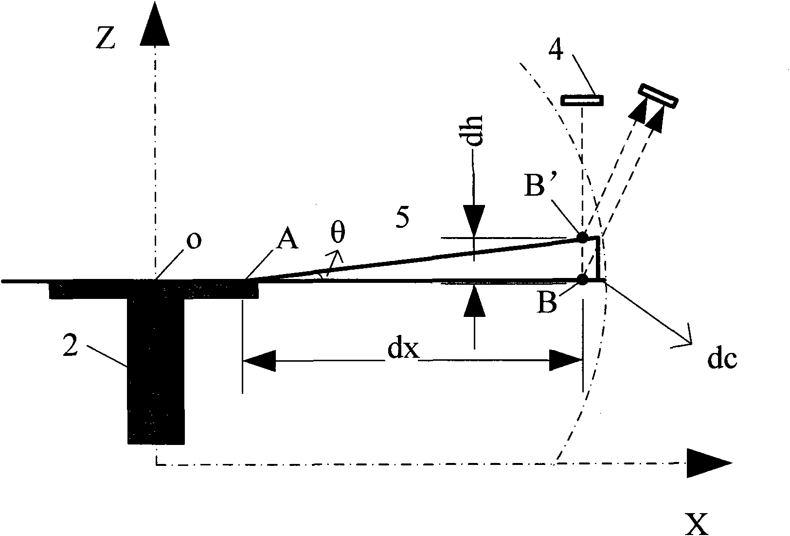
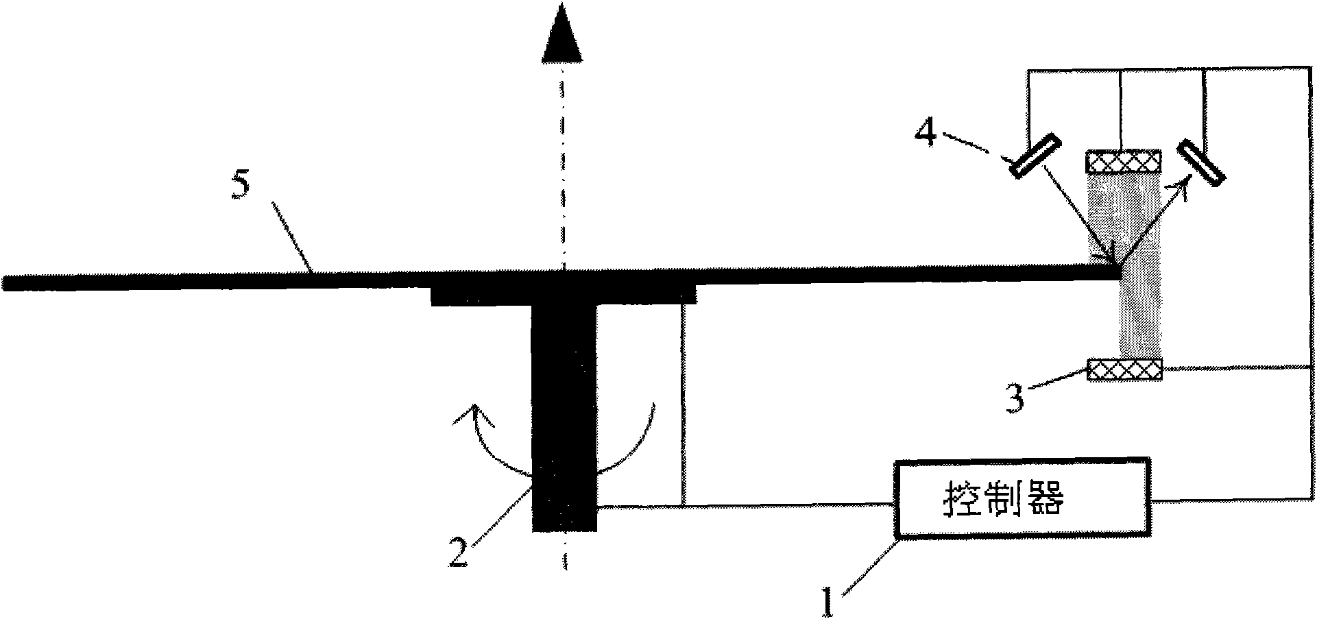
[0030] figure 1 Shown is a schematic structural view of the first embodiment of the silicon wafer pre-alignment device according to the present invention. The device consists of a controller 1 , a pre-alignment rotary table 2 , an edge horizontal sensor 3 and an edge vertical sensor 4 . The sensor is composed of a transmitting end and a receiving end, wherein the transmitting end and the receiving end can be integrated.

[0031] The controller 1 is used to synchronously control the turntable 2, the edge horizontal sensor 3 and the edge vertical sensor 4. When the turntable 2 rotates to an angle, the controller ...


PUM


Abstract

The invention discloses a silicon chip prealignment device. The silicon chip prealignment device comprises a rotating platform which is utilized for adsorbing a silicon chip and driving the silicon chip to rotate, an edge horizontal sensor which is utilized for acquiring horizontal position information of a silicon chip edge, an edge vertical sensor which is utilized for acquiring vertical position information of the silicon chip edge, and a controller which is utilized for synchronously controlling the rotating platform, the edge horizontal sensor and the edge vertical sensor. When the rotating platform rotates, the controller transmits synchronous trigger signals to the edge horizontal sensor and the edge vertical sensor, and the edge horizontal sensor and the edge vertical sensor acquire respective current measured values simultaneously and edge horizontal position information so that edge vertical position information can be acquired synchronously, wherein the current measured value which belongs to a measured point and is acquired by the edge vertical sensor is utilized for compensation of the current measured value which belongs to a silicon chip edge and is acquired by the edge horizontal sensor. Through the silicon chip prealignment device, all horizontal measured values of a silicon chip edge can be obtained when a silicon chip makes a round, and thus an eccentric value and a gap direction of the silicon chip can be determined. The invention also provides a silicon chip prealignment method.

Description

technical field [0001] The invention relates to the field of photolithography, in particular to a silicon chip pre-alignment device and method for a photolithography machine. Background technique [0002] During the production process of the lithography machine, the silicon wafer needs to be transferred to the workpiece table with high centering and orientation accuracy through the silicon wafer transmission mechanism. Since the position and direction of the silicon wafer are uncertain when placed in the wafer slot, it is necessary to pre-align the silicon wafer before the silicon wafer is transferred to the workpiece table, and the center of the silicon wafer can be determined by measuring the center of the silicon wafer. At the current position, the direction of the silicon wafer is determined by measuring the direction of the notch of the silicon wafer. [0003] The current common pre-alignment method is to measure the edge position of the silicon wafer through the senso...

Claims


Application Information

Patent Timeline
IPC IPC(8): G03F7/20G03F9/00
Inventor 蔡巍徐兵陈跃飞王端秀
Owner SHANGHAI MICRO ELECTRONICS EQUIP (GRP) CO LTD
Why Eureka
Try Eureka