Encapsulating method of high-strength chip

A chip packaging, high-strength technology, applied in the direction of electrical components, semiconductor/solid-state device manufacturing, circuits, etc., can solve the problems of reducing the service life of the chip, affecting the normal operation of the chip, and lack of stability of the chip packaging structure, so as to improve the strength and Toughness, multiple protections, and superior performance

Inactive Publication Date: 2012-04-04
常熟市广大电器有限公司
View PDF1 Cites 3 Cited by
  • Summary
  • Abstract
  • Description
  • Claims
  • Application Information

AI Technical Summary

Problems solved by technology

However, in some heavy-duty or high-speed mechanical equipment, the chip is often subjected to alternating stress or impact load, and the chip packaging structure lacks stability, which affects the normal operation of the chip and reduces the service life of the chip

Method used


Image

  • Encapsulating method of high-strength chip
  • Encapsulating method of high-strength chip

Examples


Embodiment Construction

[0015] The preferred embodiments of the present invention will be described in detail below in conjunction with the accompanying drawings, so that the advantages and features of the present invention can be more easily understood by those skilled in the art, so as to define the protection scope of the present invention more clearly.

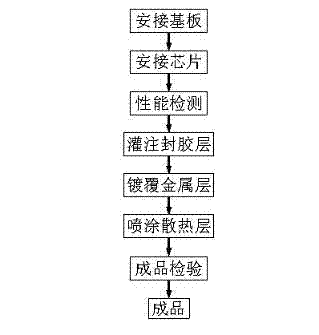
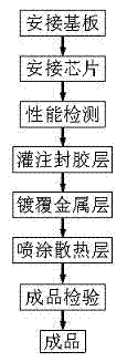
[0016] figure 1 It is a process step diagram of a high-strength chip packaging method in an embodiment of the present invention; the high-strength chip packaging method mainly includes the following steps: a) mounting the substrate, b) mounting the chip, c) performance testing, d) pouring the sealant layer, e) Plating metal layer, f) Spraying heat dissipation layer, g) Finished product inspection.

[0017] The specific implementation steps are as follows:

[0018] a) Install the substrate, the substrate is bonded to the metal pins with thermosetting adhesive, and the electrical connection with the metal pins is realized through gold wires;

[0...


PUM


Abstract

The invention discloses an encapsulating method of a high-strength chip, which mainly comprises the following steps: a) mounting and connecting a base plate, b) mounting and connecting a chip, c) detecting the performance, d) pouring a sealing layer, e) plating a metal layer, f) spraying and coating a heat dissipation layer, and g) detecting a finished product. The invention has the beneficial effects that with the adoption of the encapsulating method of the high-strength chip, the working procedures are reasonable to arrange and are easy to implement; an encapsulating body outside the chip is prepared by a plurality of working procedures in the encapsulating process to form a multi-layered encapsulating structure, thereby realizing the multiple protection to the chip and effectively improving the strength and the toughness of the encapsulating structure; and meanwhile, the good heat radiation performance of the encapsulating structure is also ensured, so that the service performance of the chip is more excellent.

Description

technical field [0001] The invention relates to a chip packaging method, in particular to a chip packaging method with high strength and excellent heat dissipation performance, and belongs to the technical field of chip packaging. Background technique [0002] In the manufacture of integrated circuits, chips are obtained through the steps of wafer fabrication, forming integrated circuits, and cutting wafers. After the integrated circuit of the wafer is fabricated, the chip formed by dicing the wafer can be electrically connected to the carrier outwardly; wherein, the carrier can be a lead frame or a substrate, and the chip can be wire bonded or covered. The method of crystal bonding is electrically connected to the carrier. If the chip and the carrier are electrically connected by wire bonding, then enter into the manufacturing step of filling the encapsulant to form the chip package. Chip packaging technology is a process technology that wraps the chip to avoid contact be...

Claims


Application Information

Patent Timeline
Patent Type & Authority Applications(China)
IPC IPC(8): H01L21/50
Inventor 徐子旸
Owner 常熟市广大电器有限公司
Why Eureka
Try Eureka