Wafer defect defection method and system

A detection method and defect technology, which are applied in the directions of optical testing defects/defects, semiconductor/solid-state device testing/measurement, etc., can solve problems such as methods and systems for determining the root cause of defects in non-defective wafers, and achieve product yield, Provides the effect of productivity

Active Publication Date: 2012-04-11
SHANGHAI HUALI MICROELECTRONICS CORP
View PDF6 Cites 16 Cited by
  • Summary
  • Abstract
  • Description
  • Claims
  • Application Information

AI Technical Summary

Problems solved by technology

[0004] So far, there is no method and system to quickly and accurately determine the root cause of defect problems based on the type of defective wafer

Method used


Image

  • Wafer defect defection method and system
  • Wafer defect defection method and system
  • Wafer defect defection method and system

Examples


Embodiment Construction

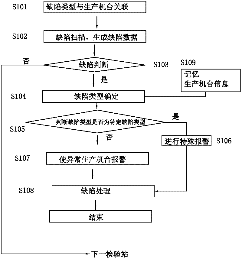
[0024] Hereinafter, specific embodiments of the present invention will be described in detail based on the drawings. The specific embodiments described here are for illustration only, and are not intended to limit the present invention.

[0025] As is well known, a wafer W which is a raw material of an IC device is manufactured through a plurality of processes such as etching and doping. The above-mentioned etching, doping and other processes are carried out on the production machine. The apparatus for processing the wafer W includes a production machine having a reaction chamber for performing the above-mentioned processing, and a robot for transferring the wafer W.

[0026] According to the number of different reaction chambers, the production machines can be divided into By1 group production machines with one reaction chamber, By2 group production machines with two reaction chambers, By3 group production machines with 3 reaction chambers, By4 group of production machines ...


PUM


Abstract

The invention provides a wafer defect detection method and system, the detection method can be used for rapidly and accurately judging reasons causing defects based on a defect style of a wafer, thereby reducing the influence of problem equipment on the product quality, and meanwhile, improving the production efficiency. The wafer defect detection method is used for a manufacture machine for respectively detecting and determining the defect on the wafer in each detection station; the detection method comprises a relevance step used for enabling the defect style to relate to each manufacture machine group respectively, a scanning step, a defect judging step, a group judging step, an alarming step and a defect processing step; and the wafer defect detection system is used for a manipulator for respectively detecting and determining the defect on the wafer in each detection station, and comprises a relevance unit used for enabling the defect style to relate to each manufacture machine group respectively, a scanning unit, a defect judging unit, a group type judging unit, an alarming unit and a defect processing unit.

Description

technical field [0001] The invention relates to a method and system for detecting wafer defects. Background technique [0002] In recent years, as the size of integrated circuit (IC) devices has been reduced, the process has become more and more complex, and accordingly, the number of machines used to produce wafers has also increased, and in order to improve production efficiency, it is necessary to shorten each The production time of the machine. However, defects will inevitably occur during the process, and being able to accurately detect defects has become a particularly important link in the entire production process. Due to the large number of production machines, the defects caused are also various, and the accurate detection of defects has become a key step that focuses on the focus and difficulty. [0003] In this case, in order to reduce the impact of problem machines on production efficiency and further improve product yield, it is particularly important to scan...

Claims


Application Information

Patent Timeline
Patent Type & Authority Applications(China)
IPC IPC(8): H01L21/66G01N21/95
Inventor 王洲男龙吟倪棋梁陈宏璘郭明升
Owner SHANGHAI HUALI MICROELECTRONICS CORP
Why Eureka
Try Eureka