

Epitaxial substrate
A technology of epitaxial substrate and epitaxial growth, which is applied in the direction of electrical components, electric solid devices, circuits, etc., can solve problems such as cracking, poor quality of epitaxial structure lattice of light-emitting diodes, restrictions on the use of silicon substrates, etc., and achieve good lattice quality , Avoid the effect of excessive accumulation of lattice stress
- Summary
- Abstract
- Description
- Claims
- Application Information
AI Technical Summary
Problems solved by technology
Method used
Image

Examples
Embodiment Construction
[0027] The embodiments of the present invention will be further described in detail below in conjunction with the accompanying drawings.
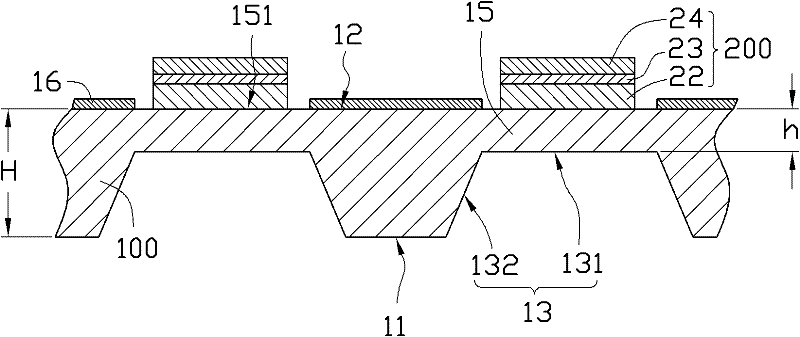
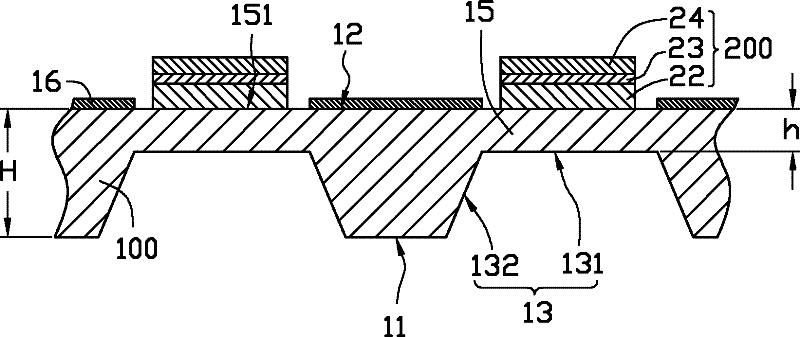
[0028] See figure 1 , The first embodiment of the present invention provides an epitaxial substrate 100 for growing a light emitting diode epitaxial structure 200. The epitaxial substrate 100 has a first surface 11 and a second surface 12 opposite thereto. The light emitting diode epitaxial structure 200 is epitaxially grown on the second surface 12 of the epitaxial substrate 100. In this embodiment, the first surface 11 is a flat surface. The material of the epitaxial substrate 100 may be silicon (Si) or silicon carbide (SiC). The distance between the first surface 11 and the second surface 12 is the thickness H of the epitaxial substrate.
[0029] The first surface 11 of the epitaxial substrate 100 has a plurality of first grooves 13 extending toward the second surface 12. In this embodiment, the plurality of first grooves 13 are arranged ...
PUM
 Abstract
Description
Claims
Application Information