Unlock instant, AI-driven research and patent intelligence for your innovation.

Method for improving data retention of SONOS (Silicon Oxide Nitride Oxide Semiconductor) and structure of SONOS

A technology of data retention and device structure, applied in the direction of electric solid-state devices, semiconductor devices, electrical components, etc., can solve the problem of hard to take out electronics, and achieve the effect of high operating voltage

Inactive Publication Date: 2012-04-18
SHANGHAI HUAHONG GRACE SEMICON MFG CORP
View PDF4 Cites 0 Cited by
  • Summary
  • Abstract
  • Description
  • Claims
  • Application Information

AI Technical Summary

Problems solved by technology

[0007] but figure 2 The disadvantages of the technical solution shown include: 1) The electrons hidden in the deep energy level are difficult to be taken out, and HOLE injection is required for erasing

Method used


Image

  • Method for improving data retention of SONOS (Silicon Oxide Nitride Oxide Semiconductor) and structure of SONOS
  • Method for improving data retention of SONOS (Silicon Oxide Nitride Oxide Semiconductor) and structure of SONOS
  • Method for improving data retention of SONOS (Silicon Oxide Nitride Oxide Semiconductor) and structure of SONOS

Examples


Embodiment Construction

[0024] In order to make the content of the present invention clearer and easier to understand, the content of the present invention will be described in detail below in conjunction with specific embodiments and accompanying drawings.

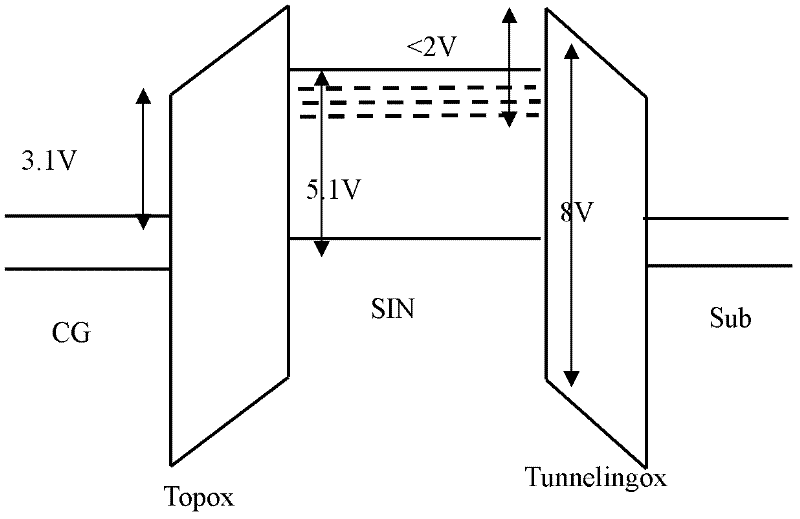
[0025] image 3 is a diagram schematically showing the structure of a SONOS device according to an embodiment of the present invention.

[0026] Specifically, for the above-mentioned problems of the prior art, in image 3 In the shown structure of the SONOS device according to the embodiment of the present invention, a composition with a high Si / N ratio is used in the silicon nitride layer SIN region near the oxide layer (top layer silicon oxide layer Top ox and tunneling silicon oxide layer Tunneling ox) (Silicon nitride layer region with high Si / N ratio), the energy band gap (Eg) of the obtained silicon nitride layer region richer in silicon is relatively low (for example, about 3.7V), so that the electrons stored therein The barrier to the ...


PUM


Abstract

The invention provides a method for improving data retention of an SONOS (Silicon Oxide Nitride Oxide Semiconductor) and a structure of the SONOS. The SONOS comprises grid silicon, a top silicon oxide layer, a silicon nitrate layer, a tunneling silicon oxide layer and a substrate silicon layer which are abutted in sequence. The method for improving the data retention of the SONOS comprises the following step of enabling a Si / N ratio of a silicon nitrate area which is close to the top silicon oxide layer and the tunneling silicon oxide layer in the silicon nitrate layer to be more than the Si / N ratio of the middle part of the silicon nitrate layer. Therefore, the data retention of the SONOS can be improved by simple improvement and a complicated process is not needed; and according to the method for improving the data retention of the SONOS, provided by the invention, a dielectric constant of the silicon nitrate layer is not increased on one hand, so that the thicker tunneling silicon oxide layer can be manufactured and the over-high operation voltage cannot be caused.

Description

technical field [0001] The present invention relates to the field of semiconductor device design, and more specifically, the present invention relates to a method for improving data retention of SONOS (silicon / silicon dioxide / silicon nitride / silicon dioxide / silicon) devices and a SONOS device structure. Background technique [0002] With the development of miniaturization and miniaturization of semiconductor storage devices, the traditional polysilicon floating gate storage is difficult to adapt to the development requirements of future storage due to the excessive thickness of the stack and the high requirements on the insulation of the tunnel oxide layer. Therefore, the SONOS (Polysilicon-Oxide-Nitride-Oxide-Silicon, silicon / silicon dioxide / silicon nitride / silicon dioxide / silicon) nonvolatile memory device based on silicon nitride with excellent insulating properties is known for its relative The traditional polysilicon floating gate memory has stronger charge storage capa...

Claims


Application Information

Patent Timeline
IPC IPC(8): H01L27/115H01L29/51
Inventor 张雄
Owner SHANGHAI HUAHONG GRACE SEMICON MFG CORP