Method for forming nickel silicide blocking layer

A technology of nickel silicide and barrier layer, which is applied in the field of forming nickel silicide barrier layer, and can solve the problem that nickel is easily oxidized

Active Publication Date: 2012-05-02
SHANGHAI HUALI MICROELECTRONICS CORP
View PDF3 Cites 2 Cited by
  • Summary
  • Abstract
  • Description
  • Claims
  • Application Information

AI Technical Summary

Problems solved by technology

[0004] The invention discloses a method for forming a nickel silicide barrier layer. The purpose of the invention is to provide a process for preventing nickel from being oxidized by oxygen in the air, so as to solve t

Method used


Image

  • Method for forming nickel silicide blocking layer
  • Method for forming nickel silicide blocking layer
  • Method for forming nickel silicide blocking layer

Examples


Embodiment Construction

[0022] The present invention will be further described below in combination with schematic diagrams and specific operation examples.

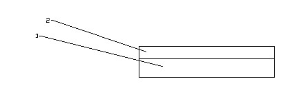
[0023] Such as Figure 1A As shown, there is a layer of first barrier metal layer 2 on the silicon substrate 1. Before forming the first barrier metal layer 2, the oxide on the surface of the silicon substrate 1 needs to be removed. The first barrier metal layer 2 covers the silicon substrate. On the bottom 1, the first barrier metal layer 2 is a silicide produced by the reaction of nickel and silicon, and the first barrier metal layer 2 may also be a silicide produced by the reaction of titanium and silicon.

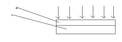
[0024] Such as Figure 1B As shown, after the first metal layer 2 is formed, a kind of gas is passed into the first metal layer 2 immediately, and this gas is a kind of gas that is difficult to react chemically with nickel, and a preferred gas in the present invention is hydrogen, Control the pressure of hydrogen to 0.01 to 1Mpa, discha...


PUM


Abstract

The invention discloses a method for forming a nickel silicide blocking layer, which mainly comprises the following steps that: the cleaning treatment is carried out on the silicon substrate surface for removing oxides on the silicon substrate surface, and a first metal layer is deposited on a silicon substrate; and the oxidation resistant treatment is carried out on the first metal layer, then, a second metal layer is deposited on the first metal layer, and the first metal layer and the second metal layer jointly form a metal blocking layer of the silicon substrate surface. The first metal layer deposited on the silicon substrate surface is nickel or NiPt, after the first metal layer is deposited on the silicon substrate surface, hydrogen gas capable of preventing the nickel from being oxidized is continuously introduced into the first metal layer surface for 1 second to 5 minutes under the conditions of the temperature being 20 DEG C to 100 DEG C and the pressure being 0.01 to 1MPa, then, the second metal layer is deposited on the first metal layer and is titanium nitride, and the first metal layer and the second metal layer jointly form the metal blocking layer of the silicon substrate surface.

Description

technical field [0001] The invention relates to the field of semiconductor integrated circuit manufacturing, and particularly relates to a method for forming a nickel silicide barrier layer. Background technique [0002] In the semiconductor processing industry, salicide formation is well known as a method of integrating low resistance materials on pre-defined areas of semiconductor structures processed to form semiconductor devices. Specifically, the salicide process is a method of reacting a silicon region of a semiconductor structure with a metal to form a silicide region. The self-aligned silicide can be selectively formed on the semiconductor structure without patterning or etching the deposited silicide, thereby forming regions of low resistance. [0003] With process scaling down to 65nm and below, nickel has been commonly used as a metal that reacts with silicon materials to form salicides on semiconductor structures. However, nickel is very active and easily react...

Claims


Application Information

Patent Timeline
IPC IPC(8): H01L21/28H01L21/283
Inventor 周军傅昶
Owner SHANGHAI HUALI MICROELECTRONICS CORP
Why Eureka
Try Eureka