

Transparent Conductive Laminated Film
A technology of transparent conductivity and laminated film, which is applied to the direction of conductive layer, coating, layered products, etc. The effect of reducing the reduction of visibility and suppressing
- Summary
- Abstract
- Description
- Claims
- Application Information
AI Technical Summary
Problems solved by technology
Method used
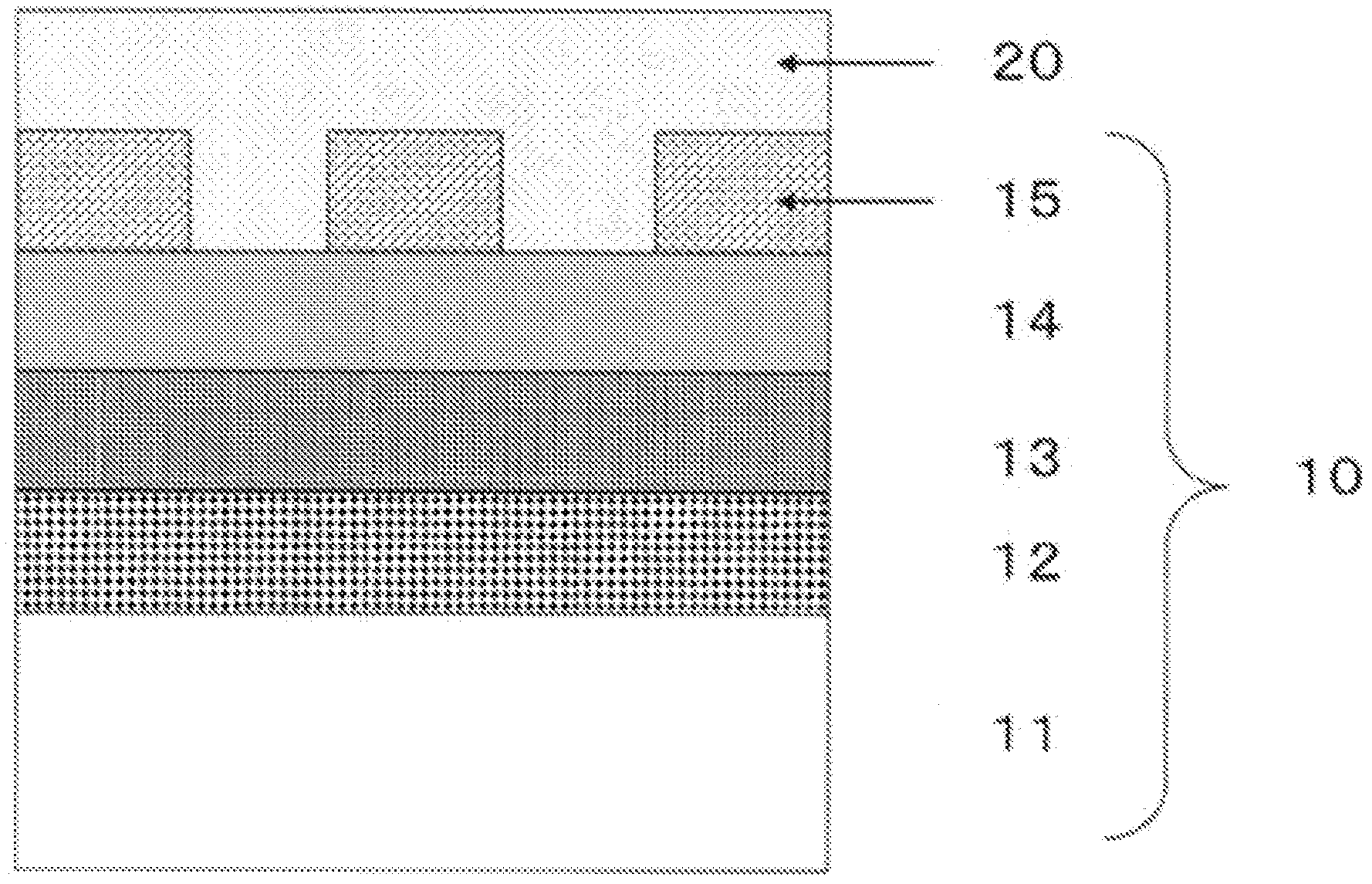
Image

Examples
Embodiment 1
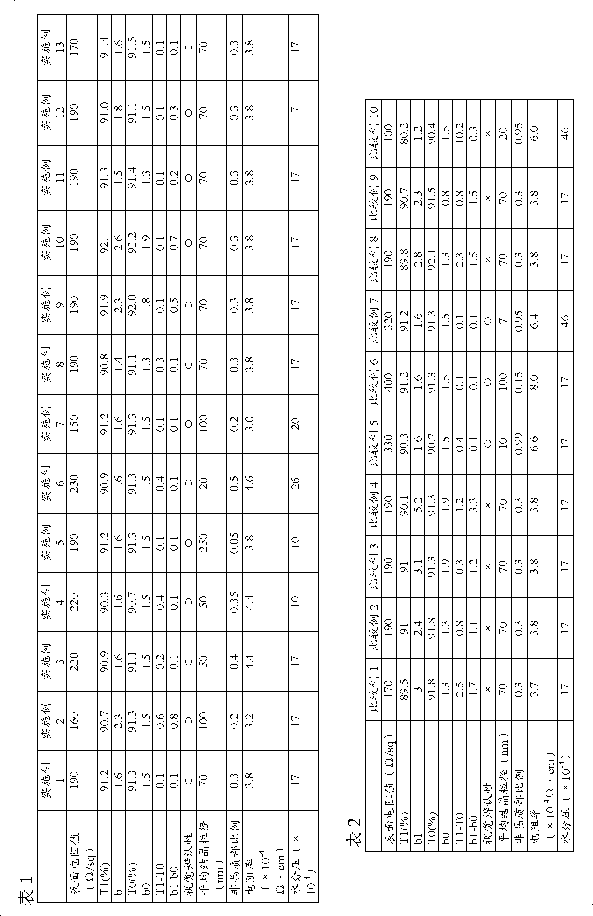
[0124] Add toluene / MEK (80 / 20: mass ratio) as a solvent to 100 parts by mass of an ultraviolet-curable acrylic (ester) resin (manufactured by Dainichi Seika Kogyo Co., Ltd., SEIKABIMU EXF-01J) containing a photopolymerization initiator and mix The solvent was adjusted to have a solid content concentration of 50% by mass, stirred and dissolved uniformly, and prepared as a coating liquid.
[0125] The prepared coating solution was applied to a biaxially oriented transparent PET film (manufactured by Toyobo Co., Ltd., A4300, thickness 100 μm) having an easy-adhesive layer on both sides with a Meyer Bar coater so that the thickness of the coating film was 5 μm. After drying at 80°C for 1 minute, irradiate ultraviolet rays (light intensity: 300mJ / cm2) with an ultraviolet irradiation device (manufactured by EYEGRAPHICS CO., LTD. 2 ) to cure the coating. Next, after preparing a coating film similarly to the opposite surface, it heated at 180 degreeC for 1 minute, and reduced the vol...
Embodiment 2
[0134] Except that the target material when forming a transparent conductive film was changed to indium oxide containing 1% by mass of tin oxide (manufactured by Sumitomo Metal Mining Co., Ltd., density 7.1g / cm 3 ) except that in the same manner as in Example 1, a transparent conductive laminated film was produced.
Embodiment 3
[0136] In addition to changing the target material when forming a transparent conductive film to indium oxide containing 5% by mass of tin oxide (manufactured by Sumitomo Metal Mining Co., Ltd., density 7.1g / cm 3 ) except that in the same manner as in Example 1, a transparent conductive laminated film was produced.
PUM
| Property | Measurement | Unit |
|---|---|---|
| thickness | aaaaa | aaaaa |
| thickness | aaaaa | aaaaa |
| electrical resistivity | aaaaa | aaaaa |
Abstract
Description
Claims
Application Information