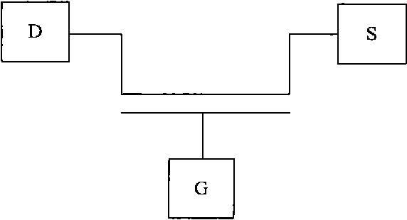
Method and device for testing characteristics of thin film transistor on array substrate
A technology of thin film transistors and array substrates is applied in the field of testing the characteristics of thin film transistors on array substrates, which can solve the problems of large deviation of real characteristics, affecting TFT-related characteristics, inaccurate test results, etc., achieving accurate test results, shortening verification time, The effect of avoiding time stress effects
- Summary
- Abstract
- Description
- Claims
- Application Information
AI Technical Summary
Problems solved by technology
Method used
Image


Examples
Embodiment Construction
[0029] The following will clearly and completely describe the technical solutions in the embodiments of the present invention with reference to the accompanying drawings in the embodiments of the present invention. Obviously, the described embodiments are only some, not all, embodiments of the present invention. Based on the embodiments of the present invention, all other embodiments obtained by persons of ordinary skill in the art without making creative efforts belong to the protection scope of the present invention.
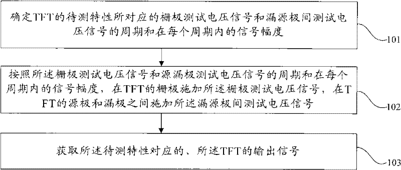
[0030] Such as image 3 As shown, the method for testing a thin film transistor on an array substrate provided in an embodiment of the present invention includes:
[0031] Step 101 , determining the period of the gate test voltage signal and the drain-source test voltage signal corresponding to the characteristics of the TFT to be tested and the signal amplitude in each period.
[0032] Wherein, the gate test voltage signal and the drain-to-source test voltag...
PUM
 Abstract
Description
Claims
Application Information
 - R&D
- Intellectual Property
- Life Sciences
- Materials
- Tech Scout
- Unparalleled Data Quality
- Higher Quality Content
- 60% Fewer Hallucinations
Browse by: Latest US Patents, China's latest patents, Technical Efficacy Thesaurus, Application Domain, Technology Topic, Popular Technical Reports.
© 2025 PatSnap. All rights reserved.Legal|Privacy policy|Modern Slavery Act Transparency Statement|Sitemap|About US| Contact US: help@patsnap.com