Embedded digital ip strip chip

A technology for configuring logic and regions, applied in the field of integrated circuits and designing integrated circuits

Active Publication Date: 2012-05-16
ALTERA CORP
View PDF7 Cites 0 Cited by
  • Summary
  • Abstract
  • Description
  • Claims
  • Application Information

AI Technical Summary

Problems solved by technology

Thus, both migration paths and embedded hard macros have disadvantages for emerging protocols because there is a balance between the need to determine migration or provide hard macros and the need for flexibility as emerging protocols evolve

Method used


Image

  • Embedded digital ip strip chip
  • Embedded digital ip strip chip
  • Embedded digital ip strip chip

Examples


Embodiment Construction

[0016] An integrated circuit having a digital strip area is provided. It will be apparent, however, to one skilled in the art that the present invention may be practiced without some or all of these specific details. In other instances, well known process operations have not been described in detail in order not to unnecessarily obscure the present invention.

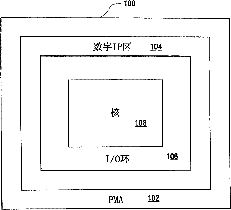
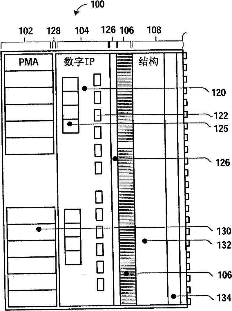
[0017] Embodiments described herein provide integrated circuits with mixed platforms. In one embodiment, an integrated circuit has a programmable logic device (PLD) core region (such as a field programmable gate array FPGA core region) and a strip or block of digital intellectual property (IP), which may also be referred to as are structured application specific integrated circuit (ASIC) strips or arrays. The digital strip includes base cells whose digital functionality can be modified by a limited number of metal masks, and standard cell macros that accommodate mature functions / protocols. In one embodiment, the digi...


PUM


Abstract

An integrated circuit (IC) is provided. The IC includes a first region having an array of programmable logic cells. The IC also includes a second region incorporated into the IC and in communication with the first region. The second region includes standard logic cells and base cells. In one embodiment, the standard logic cells are assembled or interconnected to accommodate known protocols. The base cells include configurable logic to adapt to modifications to emerging communication protocols, which are supported by the base cells. The second region can be embedded in the first region in one embodiment. In another embodiment, the second region is defined around a perimeter of the first region. The configurable logic may be composed of hybrid logic elements that have metal mask programmable interconnections so that as emerging communication protocols evolve and are modified, the IC can be modified to accommodate to the changes in the protocol. In another embodiment, a generic device can be customized by replacing the original function with a completely new function targeting a specific application space, e.g., replacing the original function such as a PCI Express, used for computing based applications, with 4OG /10OG Ethernet and Interlaken, used in wireline applications. A method of designing an integrated circuit is also provided.

Description

Background technique [0001] Programmable logic devices such as field-programmable gate arrays (FPGAs) are commonly used as prototyping platforms, but have generally been replaced by application-specific integrated circuits (ASICs), primarily due to cost and power as products are developed to high volumes . Vendors typically offer customers a migration path to prototyping in FPGAs, and then reduce cost and power by converting the design to a structured ASIC when the design is stable. In addition, once the standardization matures, hard macros (eg, PCI-Express 2.0 standard blocks) that reside directly within FPGAs representing large numbers of digital logic blocks are embedded in programmable logic devices. [0002] In either case, as emerging protocols are being developed to facilitate new high-bandwidth applications, there is a need to rapidly prototype functionality and bring viable products to market. Time to market is critical for product adoption. Cost and power are also...

Claims


Application Information

Patent Timeline
Patent Type & Authority Applications(China)
IPC IPC(8): G11C7/00G11C5/02G06F15/76
CPCH03K19/17732G06F2217/84G06F17/5045H03K19/17724G06F30/30G06F2119/12
Inventor C·沃特曼C·H·李R·G·克利夫
Owner ALTERA CORP
Why Eureka
Try Eureka