

Method of manufacturing gan-based film
A base film and axial direction technology, which is applied in chemical instruments and methods, semiconductor/solid-state device manufacturing, crystal growth, etc., can solve the problems of difficult to obtain GaN substrates and expensive GaN substrates, and achieve less warpage, large master The effect of surface area
Inactive Publication Date: 2012-05-23
SUMITOMO ELECTRIC IND LTD
View PDF4 Cites 0 Cited by
- Summary
- Abstract
- Description
- Claims
- Application Information
AI Technical Summary
Problems solved by technology
However, the GaN substrate is very expensive, and it is difficult to obtain such a GaN substrate with a large diameter whose main surface exceeds 2 inches.
Method used
View moreImage
Smart ImageViewing Examples

Examples
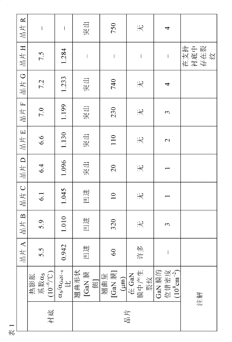
Embodiment 1
[0038] 1. Measurement of thermal expansion coefficient of GaN crystal
[0039] grown from the HVPE method and have a 1 x 10 6 cm -2 dislocation density, 1×10 18 cm -2 Si concentration, 1×10 17 cm -2 The oxygen concentration and 1 x 10 16 cm -2 A GaN single crystal cut with a carbon concentration of 2 x 2 x 20 mm for evaluation (having an a-axis in the longitudinal direction and having any one of a C plane and an M plane as a plane parallel to the longitudinal direction, And the accuracy of plane orientation is within ±0.1°).
Login to View More PUM
| Property | Measurement | Unit |
|---|---|---|
| area | aaaaa | aaaaa |
| thickness | aaaaa | aaaaa |
| thickness | aaaaa | aaaaa |
Abstract
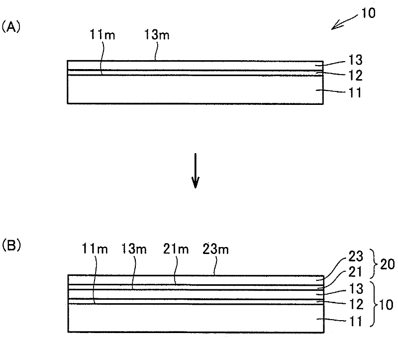
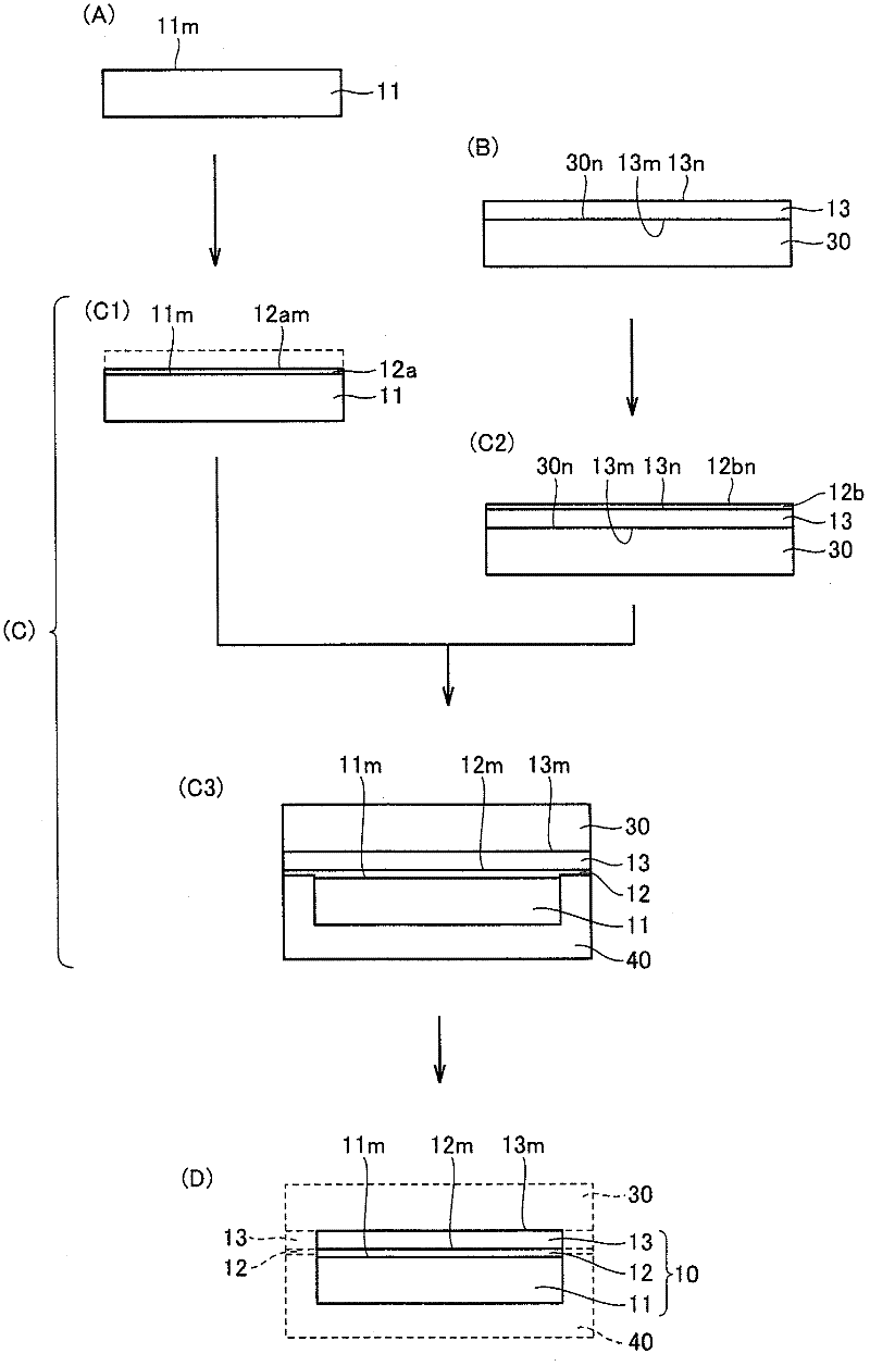
A method of manufacturing a GaN-based film includes the steps of preparing a composite substrate, the composite substrate including a support substrate in which a coefficient of thermal expansion in its main surface is more than 1.0 time and less than 1.2 times as high as a coefficient of thermal expansion of GaN crystal in a direction of a axis and a single crystal film arranged on a main surface side of the support substrate, the single crystal film having threefold symmetry with respect to an axis perpendicular to a main surface of the single crystal film, and forming a GaN-based film on the main surface of the single crystal film in the composite substrate, the single crystal film in the composite substrate being an SiC film. Thus, a method of manufacturing a GaN-based film capable of manufacturing a GaN-based film having a large main surface area and less warpage is provided.
Description
technical field [0001] The present invention relates to a method of manufacturing a GaN base film capable of obtaining a GaN base film with a large main surface area and less warpage. Background technique [0002] GaN-based films are suitable for use as substrates and semiconductor layers in semiconductor devices such as light-emitting devices and electronic devices. Considering the matching or basic matching between the substrate and the GaN base film in terms of lattice constant and thermal expansion coefficient, the GaN substrate is the best as a substrate for manufacturing such a GaN base film. However, a GaN substrate is very expensive, and it is difficult to obtain such a GaN substrate having a large diameter whose main surface exceeds 2 inches in diameter. [0003] Therefore, a sapphire substrate is generally used as a substrate for forming a GaN-based film. A sapphire substrate and a GaN crystal are significantly different from each other in lattice constant and th...
Claims
Login to View More Application Information
Patent Timeline
 Patent Type & AuthorityApplications(China)
IPC IPC(8): C30B29/38H01L21/20
CPCC30B25/18C30B29/406H01L21/0262H01L21/02458H01L21/0254C30B25/02H01L21/02378H01L33/007H01L21/02658
Inventor藤原伸介上松康二山本喜之佐藤一成
OwnerSUMITOMO ELECTRIC IND LTD