

METHOD OF MANUFACTURING GaN-BASED FILM
- Summary
- Abstract
- Description
- Claims
- Application Information
AI Technical Summary
Benefits of technology
Problems solved by technology
Method used
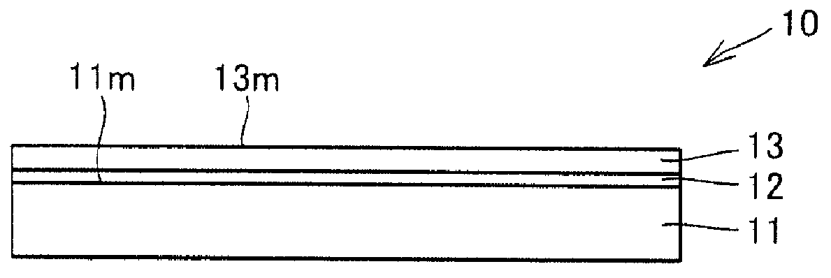
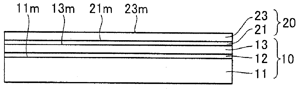
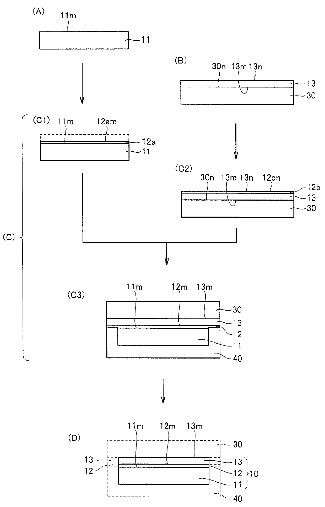
Image

Examples
example 1
1. Measurement of Coefficient of Thermal Expansion of GaN Crystal
[0039]A sample for evaluation having a size of 2×2×20 mm (having a axis in a longitudinal direction and having any of a C plane and an M plane as a plane in parallel to the longitudinal direction, with accuracy in plane orientation being within)±0.1° was cut from GaN single crystal grown with the HVPE method and having dislocation density of 1×106 cm−2, Si concentration of 1×1018 cm−2, oxygen concentration of 1×1017 cm−2, and carbon concentration of 1×1016 cm−2.
[0040]An average coefficient of thermal expansion of the sample for evaluation above when a temperature was increased from room temperature (25° C.) to 800° C. was measured with TMA (thermomechanical analysis). Specifically, using TMA8310 manufactured by Rigaku Corporation, the coefficient of thermal expansion of the sample for evaluation was measured with differential dilatometry in an atmosphere in which a nitrogen gas flows. An average coefficient of thermal ...
PUM
 Abstract
Description
Claims
Application Information