Semiconductor structure and making method thereof

A manufacturing method and semiconductor technology, applied in the direction of semiconductor/solid-state device manufacturing, semiconductor devices, semiconductor/solid-state device components, etc., can solve the problems of large cross-sectional area of ​​the second contact hole, unfavorable area saving, etc., to achieve the benefit of process design, The effect of saving area and reducing the process window

Active Publication Date: 2012-05-23
INST OF MICROELECTRONICS CHINESE ACAD OF SCI
View PDF6 Cites 9 Cited by
  • Summary
  • Abstract
  • Description
  • Claims
  • Application Information

AI Technical Summary

Problems solved by technology

[0004] However, the above-mentioned second dielectric layer 126 is relatively thick, so a larger area should be reserved when etching the second contact hole, and the cross-sectional area of ​​the second contact hole formed is also relatively large, which is not conducive to saving area.

Method used


Image

  • Semiconductor structure and making method thereof
  • Semiconductor structure and making method thereof
  • Semiconductor structure and making method thereof

Examples


Embodiment 1

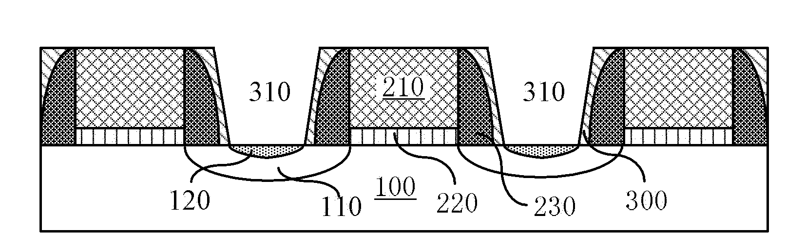
[0060] Please refer to Figure 10 to Figure 12 . The semiconductor structure includes a substrate 100, a gate stack, a spacer 230 (this document only explicitly shows an example of a semiconductor structure including a sidewall 230, but in other embodiments, the sidewall 230 may not be included), a first dielectric layer 300 , the first contact plug 320, the cover layer 400, the second contact plug 420, the second dielectric layer 500, the third contact plug 520 and each lining layer (such as the metal lining layer, the first lining layer and the second lining layer, the figure is not shown), wherein the source / drain region 110 is formed in the substrate 100; the gate stack is formed on the substrate 100, and the sidewall 230 is formed at the sidewall of the gate stack; the first dielectric layer 300 covers the source / drain region 110, the cover layer 400 covers the gate stack and the first dielectric layer 300, the first contact plug 320 penetrating through the first dielect...

Embodiment 2

[0069] On the basis of the description of the same part in the reference embodiment one, refer to Figure 16 to Figure 20 , the second contact plug 420 includes two types, one is the second contact plug 420a electrically connected to the gate metal 210 of the gate stack, and the other is the second contact plug 420b electrically connected to the first contact plug 320, by Figure 16 It can be seen that the second contact plug 420a is not on the same straight line as the two adjacent second contact plugs 420b. refer to Figure 17 to Figure 20 One or more second contact plugs 420a electrically connected to the gate metal 210 on the semiconductor structure and the two adjacent second contact plugs 420b electrically connected to the source / drain region 110 are not on the same straight line, which is also an embodiment The difference between the second embodiment and the first embodiment is that the advantage of this arrangement is that the second contact plug 420a and the second ...

Embodiment 3

[0072] On the basis of referring to the description of the same part in embodiment one or embodiment two, please refer to Figure 21 to Figure 23 . In certain cases, it is necessary to electrically connect the gate of a semiconductor structure to its source and drain, or to electrically connect the gate or source and drain of one semiconductor structure to the gate or source and drain of another nearby semiconductor structure. Such metal interconnections can be realized locally in the cap layer 400 . For example, according to the design requirements, the electrical connection between the gate and its source and drain is made, such as Figure 22 As shown, the size and shape of the second contact plug 420 in the capping layer 400 can be adjusted so that it is electrically connected to the first contact plug 320 connected to the source / drain region 110 and the gate metal 210 at the same time. The advantage of setting the second contact plug 420 in this way is to realize the ele...


PUM


Abstract

The invention discloses a semiconductor structure which comprises a first interlayer structure, a second interlayer structure and a third interlayer structure. The first interlayer structure comprises a first dielectric layer and a first contact plug, the first dielectric layer is flush with a grid stack or covers the grid stack, and the first contact plug passes through the first dielectric layer and is electrically connected with at least part of a source / drain region; the second interlayer structure comprises a cover layer and a second contact plug, the cover layer covers the first interlayer structure, and the second contact plug passes through the cover layer and is electrically connected with the first contact plug and the grid stack through a first lining; and the third interlayer structure comprises a second dielectric layer and a third contact plug, the second dielectric layer covers the second interlayer structure, and the third contact plug passes through the second dielectric layer and is electrically connected with the second contact plug through a second lining. The invention also provides a making method for the semiconductor structure. With the adoption of the semiconductor structure and the making method thereof, area saving is facilitated to improve the integration degree of the semiconductor structure.

Description

technical field [0001] The invention relates to the field of semiconductor manufacturing, in particular to a semiconductor structure and a manufacturing method thereof. Background technique [0002] With the development of semiconductor structure manufacturing technology, integrated circuits with higher performance and stronger functions require greater component density, and the size, size and space of each component, between components or each component itself need to be further reduced (currently can reach the nanoscale), with the reduction of the size of semiconductor devices, various microscopic effects are highlighted. In order to meet the needs of device development, those skilled in the art have been actively exploring new manufacturing processes. [0003] In order to solve the above problems, the US patent application US2009 / 0321942 A1 in the prior art provides a method for forming contact holes (see Figure 29 ), including: etching the first dielectric layer to for...

Claims


Application Information

Patent Timeline
Patent Type & Authority Applications(China)
IPC IPC(8): H01L21/768H01L21/8234H01L23/522H01L23/528
CPCH01L23/5226H01L2924/0002H01L29/401H01L21/76895H01L27/088H01L23/485H01L21/76807H01L21/76897H01L21/28518H01L21/76816H01L29/40114H01L2924/00
Inventor 尹海洲骆志炯朱慧珑
Owner INST OF MICROELECTRONICS CHINESE ACAD OF SCI
Why Eureka
Try Eureka