Grating coupler and coupling structure and packaging structure of grating coupler and optical fibers

A technology of grating coupler and coupling structure, which is applied in the coupling of optical waveguide and other directions, and can solve the problems of optical fiber alignment and positioning that have not been effectively solved.

Active Publication Date: 2012-05-30
NAT CENT FOR ADVANCED PACKAGING
View PDF4 Cites 33 Cited by
  • Summary
  • Abstract
  • Description
  • Claims
  • Application Information

AI Technical Summary

Problems solved by technology

[0005] At present, the coupling between the grating coupler on the SOI substrate and the optical fiber generally adopts the way that the optical fiber is coupled from the upper surface of the SOI substrate; for ordinary symmetrical g

Method used


Image

  • Grating coupler and coupling structure and packaging structure of grating coupler and optical fibers
  • Grating coupler and coupling structure and packaging structure of grating coupler and optical fibers
  • Grating coupler and coupling structure and packaging structure of grating coupler and optical fibers

Examples


Embodiment 1

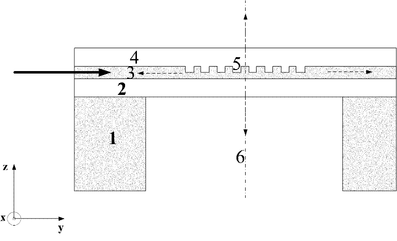
[0021] Such as figure 1 As shown, the schematic diagram of the basic structure of the grating coupler with silicon substrate layer etching holes provided by the embodiment of the present invention;

[0022] The grating coupler on the SOI substrate is: the silicon substrate layer 1 of the SOI substrate, the silicon dioxide intermediate layer 2 of the SOI substrate from bottom to top, the silicon top layer 3 of the SOI substrate and the upper cladding layer 4 to form a vertical optical The waveguide structure, the optical coupling grating 5 located on the silicon top layer 3 of the SOI substrate, and the etching hole 6 are etched on the silicon substrate layer 1 of the SOI substrate. The etching hole 6 is formed by dry etching. During the dry etching process, the silicon dioxide intermediate layer 2 of the SOI substrate becomes an etching stopper layer, that is, the etching hole 6 passes through the silicon substrate layer 1 of the SOI substrate. It ends at the lower surface of...

Embodiment 2

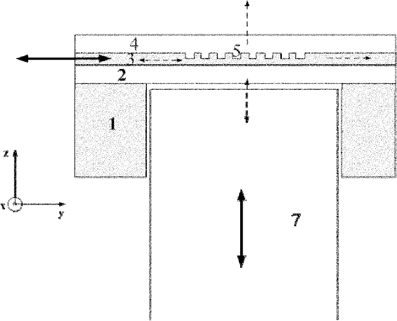
[0024] Such as figure 2 As shown, the embodiment of the present invention provides a schematic diagram of the coupling structure of the grating coupler with the silicon substrate layer etching hole and the optical fiber;

[0025] The grating coupler on the SOI substrate is that the silicon substrate layer 1 of the SOI substrate, the silicon dioxide intermediate layer 2 of the SOI substrate from bottom to top, the silicon top layer 3 of the SOI substrate and the upper cladding layer 4 constitute a vertical optical The waveguide structure, and the optical coupling grating 5 located on the silicon top layer 3 of the SOI substrate, and the silicon substrate layer 1 of the SOI substrate are etched with an etching hole 6, and the axis of the etching hole 6 coincides with the center of the optical coupling grating 5 Inserting the optical fiber 7 into the etched hole 6 realizes the self-alignment and positioning of the optical coupling grating and the optical fiber. The positioning ...

Embodiment 3

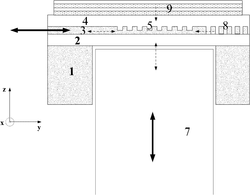
[0027] Such as image 3 As shown, the embodiment of the present invention provides a grating coupler with a silicon substrate layer etching hole, a back grating and a top grating, and a schematic diagram of its coupling structure with an optical fiber;

[0028] In order to reduce the light energy leakage loss along the back direction after the light wave is diffracted by the optical coupling grating 5 in the optical waveguide structure and the light energy leakage loss that is emitted upward after the light wave is diffracted by the optical coupling grating 5, the designed silicon substrate layer engraved grating coupler for pitting, back grating and top grating,

[0029] The grating coupler on the SOI substrate is that the silicon substrate layer 1 of the SOI substrate, the silicon dioxide intermediate layer 2 of the SOI substrate from bottom to top, the silicon top layer 3 of the SOI substrate and the upper cladding layer 4 constitute a vertical optical The waveguide struct...


PUM


Abstract

The invention discloses a grating coupler, which comprises a silicon substrate layer (1) of a silicon-on-insulator (SOI) substrate, an optical waveguide structure and an optical coupling grating (5). The optical waveguide structure consists of a silicon dioxide intermediate layer (2) of the SOI substrate, a silicon top layer (3) of the SOI substrate and an upper cladding layer (4) from the bottom up. The optical coupling grating (5) is arranged on the silicon top layer (3) of the SOI substrate. An etched hole (6) is etched on the silicon substrate layer (1) of the SOI substrate. The invention additionally discloses a coupling structure of the grating coupler and optical fibers and a packaging structure for coupling of the grating coupler and the optical fibers. By using the grating coupler, the coupling structure and the packaging structure, the passive self-alignment and positioning of the optical coupling grating and the optical fibers can be realized.

Description

technical field [0001] The invention relates to the fields of optical communication and optical interconnection, in particular to a grating coupler on an SOI substrate, a coupling structure with an optical fiber, and a packaging structure. Background technique [0002] With the explosive development of the global digitalization process, information technology places more emphasis on low power consumption, high bandwidth density and low cost. Integration of discrete optoelectronic devices, automated mass production and low-cost assembly is a promising solution. III-V materials have always occupied a dominant position in the field of optoelectronic devices, but due to the inherent characteristics and process limitations of materials, different photonic devices are fabricated on different material substrates (such as InP, GaAs, lithium niobate, etc.) , the integration is very difficult, the integration level is low, the cost is expensive, and the process compatibility with the...

Claims


Application Information

Patent Timeline
IPC IPC(8): G02B6/34
Inventor 李宝霞
Owner NAT CENT FOR ADVANCED PACKAGING
Why Eureka
Try Eureka