Semiconductor substrate and preparation method thereof

A technology for semiconductors and substrates, applied in the field of semiconductor substrates and their manufacturing methods to avoid cracking of solder balls, can solve problems such as local melting, lower yield, difficulty in opening holes 150 and filling them completely, and achieve the effect of avoiding falling off or cracking

Active Publication Date: 2012-06-06
SILICONWARE PRECISION IND CO LTD
View PDF6 Cites 8 Cited by
  • Summary
  • Abstract
  • Description
  • Claims
  • Application Information

AI Technical Summary

Problems solved by technology

[0007] However, since the solder 160 is formed by brushing, it is not easy to fill the opening 150 completely, so that after the reflow soldering manufacturing method, the solder ball 16' is prone to voids, And it is easy to cause local melting (local melting) of the solder ball 16' due to electro migration (EM), so that the electrical contact pad 100' cannot be effectively connected when the subsequent flip chip (flipchip) manufacturing method is performed. to the packaging substrate, and thus cannot effectively produce electrical connections, thus reducing the yield of the product

Method used


Image

  • Semiconductor substrate and preparation method thereof
  • Semiconductor substrate and preparation method thereof
  • Semiconductor substrate and preparation method thereof

Examples


Embodiment Construction

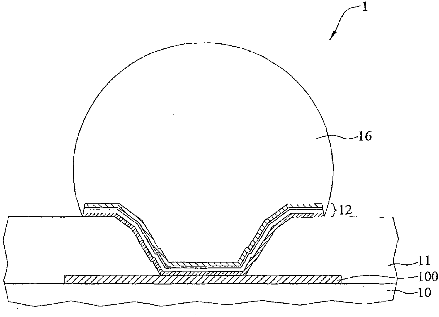
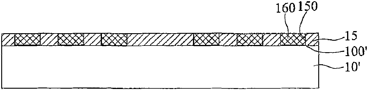
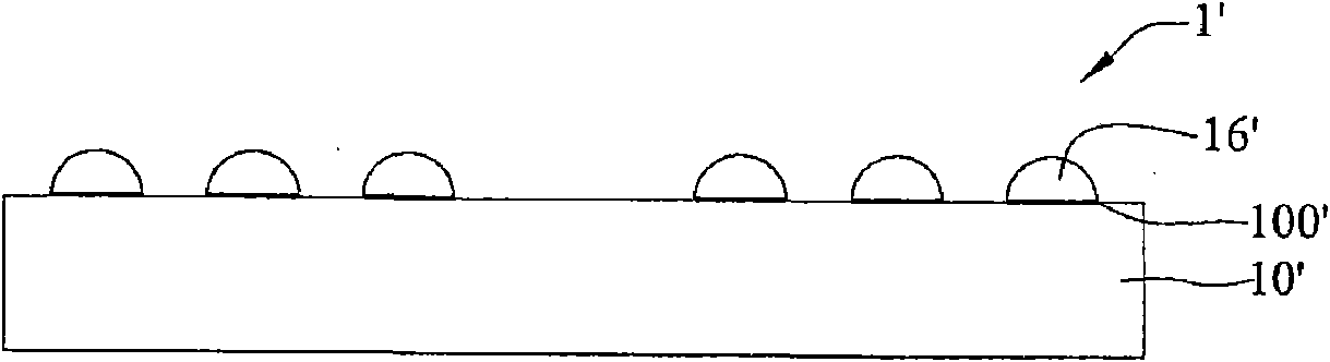
[0041] The following specific examples illustrate the implementation of the present invention. Those skilled in the art can easily understand other advantages and effects of the present invention from the content disclosed in this specification.

[0042] It should be understood that the structures, proportions, sizes, etc. shown in the accompanying drawings in this specification are only used to match the contents disclosed in the specification for the understanding and reading of those skilled in the art, and are not intended to limit the implementation of the present invention. Therefore, it does not have technical significance. Any structural modification, proportional relationship change or size adjustment, without affecting the effects and objectives that can be achieved by the present invention, should still fall under the original The technical content disclosed by the invention must be within the scope covered. At the same time, terms such as "上", "一" and "下" cited in thi...


PUM


Abstract

The invention relates to a semiconductor substrate and a preparation method thereof. The semiconductor substrate comprises a substrate, a first insulating protective layer, a metal layer, a second insulating protective layer, and a solder ball. More particularly, an electrical contact pad is arranged on the surface of the substrate; the first insulating protective layer is arranged on the substrate and enables the electrical contact pad to be exposed; the metal layer is arranged on the exposed electrical contact pad; the second insulating protective layer is arranged on the first insulating protective layer and enables a portion of the metal layer to be exposed; and the solder ball is arranged on the exposed metal layer. Because the second insulating protective layer is covered on a portion of the metal layer, when a temperature test is carried out on the semiconductor substrate, problems that the solder ball drops off or fractures and the like can be solved. Furthermore, the invention also provides a preparation method of the semiconductor substrate.

Description

Technical field [0001] The invention relates to a semiconductor substrate and a manufacturing method thereof, in particular to design a semiconductor substrate and a manufacturing method thereof to avoid cracking of solder balls. Background technique [0002] With the vigorous development of the electronics industry, electronic products have gradually entered the direction of multi-functional and high-performance research and development. The current design of semiconductor chips includes wire bonding and flip chip, etc., to connect the chip on the package substrate, and set a gold wire or conductive bump between the chip and the package substrate. Block to electrically connect the chip to the packaging substrate. [0003] In order to achieve multiple functions, high operating power, and long service life, the electrical stability of the chip is very important. Refer to US Patent No. 6,107,180 or US 6,111,321, or refer to figure 1 , Is a schematic cross-sectional view of an exist...

Claims


Application Information

Patent Timeline
Patent Type & Authority Applications(China)
IPC IPC(8): H01L23/00H01L21/60
CPCH01L24/11H01L2224/11H01L2924/00012
Inventor 简丰隆陈宜兴郭夔孝
Owner SILICONWARE PRECISION IND CO LTD
Why Eureka
Try Eureka