Single instruction multiple data (SIMD) vector processor supporting fast Fourier transform (FFT) acceleration

A vector processor and vector operation technology, applied in electrical digital data processing, instruments, memory systems, etc., can solve problems such as on-chip resource occupation, avoid hardware overhead, and ensure performance.

Inactive Publication Date: 2012-06-13
NANJING UNIV
2 Cites 10 Cited by

AI-Extracted Technical Summary

Problems solved by technology

SIMD vector processors can be used to accelerate regular vector operations, but there is no SIMD vector processor that can directly accelerate FFT operations at the same time (acceleration efficiency is compa...

Abstract

The invention discloses a single instruction multiple data (SIMD) vector processor supporting fast Fourier transform (FFT) acceleration, which comprises a control unit, a calculation unit, a storage subsystem, a storage weaving unit and an address generation unit. The calculation unit supports quick processing of various vector calculations. The storage subsystem comprises three storage groups. Each storage group comprises four storage bodies, the bit wide of a single storage body in each storage group is a plural character, and the storage groups support plural vector calculation with concurrent four-way data and real number vector calculation with concurrent eight-way data. The calculation unit, the address generation unit and the storage weaving unit are connected with the control unit. The address generation unit generates required operand address sequence, coefficient address sequence and result address sequence. The storage weaving unit and the address generation unit are connected with the calculation unit to achieve address mapping of the storage bodies. The acceleration efficiency of the SIMD vector processor to FFT/ inverse fast Fourier transform (IFFT) calculation corresponds to a special hardware accelerator. The SIMD vector processor avoids huge extra pay expenses brought by use of the special hardware accelerator, and is suitable for being used in a real-time signal processing system with a large amount of long vector calculation.

Application Domain

Technology Topic

Hardware accelerationAddress mapping +10

Image

  • Single instruction multiple data (SIMD) vector processor supporting fast Fourier transform (FFT) acceleration
  • Single instruction multiple data (SIMD) vector processor supporting fast Fourier transform (FFT) acceleration
  • Single instruction multiple data (SIMD) vector processor supporting fast Fourier transform (FFT) acceleration

Examples

  • Experimental program(1)

Example Embodiment

[0017] The SIMD vector processor supporting FFT acceleration of the present invention will be described in detail below with reference to the accompanying drawings.
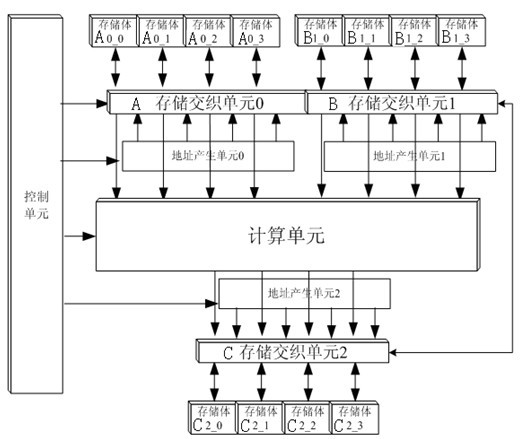
[0018] A SIMD vector processor that supports FFT acceleration, see figure 1 The processor includes a control unit, a calculation unit, a memory subsystem, a storage interleaving unit and an address generation unit.
[0019] The calculation unit supports fast processing of various vector operations. The calculation unit includes 2 complex multipliers and 4 complex adders. It supports 2 data parallel complex multiplication and convolution operations, and 4 data parallel complex addition and subtraction, accumulation Operation, 4 data parallel complex modulus operations, 4 data parallel FFT/IFFT operations, and 8 data parallel real number multiplication, convolution, addition and subtraction, accumulation operations. For the aforementioned n-way data parallel vector operation, n vector units are processed on average per clock cycle (without considering the pipeline filling time before each vector is processed). Its acceleration efficiency is equivalent to that of a dedicated hardware accelerator and supports variable points. Therefore, while ensuring the calculation efficiency of the system, it saves the huge amount of on-chip storage resources and logic resource overhead caused by the use of FFT dedicated hardware acceleration units in the design.
[0020] The memory subsystem includes three memory groups, namely memory group A for storing operands, memory group B for storing coefficients, and memory group C for storing calculation results, and each memory group contains 4 memory banks. The bit width of a single memory bank is a complex number, which supports 4-way data parallel complex number vector operation and 8-way data parallel real number vector operation, so that the 4 operands read at the same time are located in 4 different banks and written at the same time The input 4 operation results are located in 4 different memory banks; through the programmable address mapping method, it supports regular vector operations and FFT/IFFT operations of various length vectors. The calculation unit, the address generation unit and the storage interleaving unit are all connected to the control unit.
[0021] The address generation unit generates the required operand address sequence, coefficient address sequence, and result address sequence according to the type of operation, the data parallelism of the operation, and the length of the vector; the storage interleaving unit is connected with the address generation unit and the calculation unit, and realizes the storage volume Address mapping. The storage interleaving unit is adapted to the three memory banks and also includes three parts: storage interleaving unit A, storage interleaving unit BT and storage interleaving unit C.
[0022] The programmable address mapping method is to set the vector length through software programming. For different vector lengths, the address mapping method also changes accordingly, and under each vector length, it can ensure that the regular vector operation and FFT/IFFT operation are conflict-free. .
[0023] As mentioned earlier, the biggest obstacle to enabling SIMD processors that support regular vector operations to support FFT direct acceleration lies in address conflicts. This problem is also faced in the design of FFT dedicated hardware accelerators, and there are already mature solutions, which can generally be avoided by designing storage systems and address mapping flexibly. However, the problem is more complicated here, because it is necessary to support the acceleration of other regular vector operations after adding FFT acceleration instructions.
[0024] The present invention applies the new radix-2 DIT FFT operation data flow diagram, and proposes an address mapping method that supports both regular vector operation and FFT/IFFT conflict-free memory access, and its programmability supports various length vectors Operation.
[0025] figure 2 It is a traditional radix-2 DIT FFT operation data flow diagram (input data has undergone address bit inversion). When calculating based on this data flow graph, the address sequence of the operand is the same as the address sequence of the result, but the address sequence for each level of operation is different, see Table 1.
[0026] Table 1 Address sequence of each operand/result data channel (for FFT of length 8)
[0027]
[0028] The address mapping of the original SIMD vector processor is shown in Table 2
[0029] Table 2 Address mapping of the original SIMD vector processor
[0030]
[0031] It can be seen that there is an address conflict in the second level. The addresses of the two operands of butterfly operation 2_0 are 0 and 4 respectively, and they are both in bank_0. The addresses of the two operands of butterfly operation 2_1 are respectively 1 and 5, which are all in bank_1, the addresses of the two operands of butterfly operation 2_2 are 2, and 6, both are in bank_2, and the addresses of the two operands of butterfly operation 2_3 are respectively 3 and 7, both are in bank_7.
[0032] You can avoid address conflicts by simply changing the address mapping. However, for an FFT with a length greater than 8, there are address conflicts at each level from the third level onwards, and more importantly, because the address sequence of each level is different, the conflicting addresses of each level are different. Moreover, changing the address mapping may also cause address conflicts in regular vector operations, so this problem cannot be solved by simply changing the address mapping.
[0033] There is a new radix-2 DIT FFT operation data flow diagram, its address sequence is the same for each level of butterfly operation, such as image 3 Shown. The new radix-2 DIT FFT operation data flow graph is a change from the traditional radix-2 DIT FFT operation data flow graph. In the traditional radix-2 DIT FFT operation data flow diagram, the 0th level has N/2 groups, each group has 1 butterfly operation; the first level has N/4 groups, each group has 2 butterfly operations; the second level There are N/8 groups, each group has 4 butterfly operations; and so on.
[0034] At each level, the calculation sequence of butterfly operations is: complete each group of operations from top to bottom, and in each group, each butterfly operation is also performed from top to bottom. If you adjust the calculation order of the butterfly operation above: first calculate the first butterfly operation of each group from top to bottom, and then calculate the second butterfly operation of each group from top to bottom, and so on until Complete all butterfly operations at this level. Taking N=8 FFT as an example, according to the traditional radix-2 DIT FFT operation data flow diagram, the butterfly operation order of the first stage is 1_0 -> 1_1 -> 1_2 -> 1_3, and the adjusted butterfly operation order is 1_0 -> 1_2 -> 1_1 -> 1_3. According to the adjusted butterfly operation sequence, and according to the new calculation sequence, the data stored in the memory location is adjusted accordingly, then we get image 3 The new radix-2 DIT FFT operation data flow diagram shown.
[0035] When calculating based on the new radix-2 DIT FFT operation data flow diagram, the address sequence of the operand is different from the address sequence of the result, but the address sequence is the same for each level of operation, see Table 3 and Table 4.
[0036]
[0037] Table 3 Data channel address sequence of each operand (based on the new radix-2 DIT FFT operation data flow diagram)
[0038]
[0039] Table 4 The address sequence of each result data channel (based on the new radix-2 DIT FFT operation data flow diagram)
[0040]
[0041] It can be seen from Table 3 that the address sequence of the operand is the same as that of the rule vector operation, and there is no address conflict. It can be seen from Table 4 that the address sequence of the result always has an address conflict. For example, the addresses of the two results of butterfly operation 0_0 are 0 and 4 respectively, and they are both in bank_0. This problem can be solved by changing the address mapping, as long as it is ensured that the changed address mapping will not cause address conflicts in the address sequence of the rule vector operation.
[0042] For the vector with N=8, it can be changed to the address mapping shown in Table 5.
[0043] Table 5 New address mapping (for N=8 vector)
[0044]
[0045] According to the address mapping in Table 5, the address sequences in Table 3 and Table 4 are conflict-free, so the parallel memory access for regular vector operations and N=8 FFT operations are conflict-free. The SIMD vector processor can support these at the same time. Operational acceleration.
[0046] Generalized to any vector length N, the address mapping is shown in Table 6
[0047] Table 6 Address mapping for any vector length N
[0048]
[0049] In this way, for vectors of any length N, the SIMD vector processor can support the direct acceleration of regular vector operations and FFT/IFFT operations. It can be seen from Table 6 that the address mapping is related to the vector length N. In the designed SIMD vector processor, the address mapping is implemented by the memory interleaving unit. Therefore, before the vector is loaded from the off-chip memory to the on-chip memory, the vector length needs to be set to the memory interleaving unit by software programming. Load the vector to the on-chip memory and perform a series of accelerated operations on the vector, including regular vector operations and FFT/IFFT operations. Therefore, this address mapping method is called programmable address mapping.
[0050] The FFT acceleration performance in this embodiment is an average of two butterfly operations per clock cycle, and the acceleration efficiency (the number of butterfly operations per cycle/the number of complex multipliers) reaches the highest, which is 1, and the maximum of the dedicated hardware accelerator The acceleration efficiency is comparable.
[0051] In addition, it should be particularly noted that the design method of the present invention has great scalability, the degree of parallelism can be selected according to performance requirements, and the number of butterfly operations in parallel computing can be selected as 1, 2, 4, 8.... The general radix-2 FFT hardware accelerator has a parallelism of 1 or log2N, and does not have the flexibility of choice, so this scalability is of great significance.
[0052] The invention can enhance the flexibility of the system under the premise of ensuring the operating efficiency of the system, and at the same time reduce the huge hardware overhead caused by the use of the FFT dedicated hardware unit, so it has excellent application value in the signal processing system.

PUM

no PUM

Description & Claims & Application Information

We can also present the details of the Description, Claims and Application information to help users get a comprehensive understanding of the technical details of the patent, such as background art, summary of invention, brief description of drawings, description of embodiments, and other original content. On the other hand, users can also determine the specific scope of protection of the technology through the list of claims; as well as understand the changes in the life cycle of the technology with the presentation of the patent timeline. Login to view more.

Similar technology patents

Classification and recommendation of technical efficacy words

Why Eureka
Try Eureka