Optical element surface defect detecting system based on active laser beam scanning

A technology of optical components and detection systems, applied in the field of optoelectronics, can solve the problems of online monitoring of surface defects of large-diameter optical components, complex application environments, and damage of monitoring equipment, etc., to overcome environmental adaptability problems and simple system structure , the effect of taking up less space

Active Publication Date: 2012-06-20
LASER FUSION RES CENT CHINA ACAD OF ENG PHYSICS
View PDF6 Cites 10 Cited by
  • Summary
  • Abstract
  • Description
  • Claims
  • Application Information

AI Technical Summary

Problems solved by technology

However, because the high-power solid-state laser device has a complex application environment, on the one hand, the interior of the optical transmission channel is mostly irradiated with strong light or high vacuum; In the light area, the use of surface defect detection equipment in such an environment is difficult to install the equipment, and secondly, improper use will easily pollute the laser device and cause damage to the monitoring equipment.
The above methods are difficult to meet the actual needs of on-line monitoring of surface defects of large-aperture optical components in high-power solid-state laser devices

Method used


Image

  • Optical element surface defect detecting system based on active laser beam scanning
  • Optical element surface defect detecting system based on active laser beam scanning

Examples


Embodiment 1

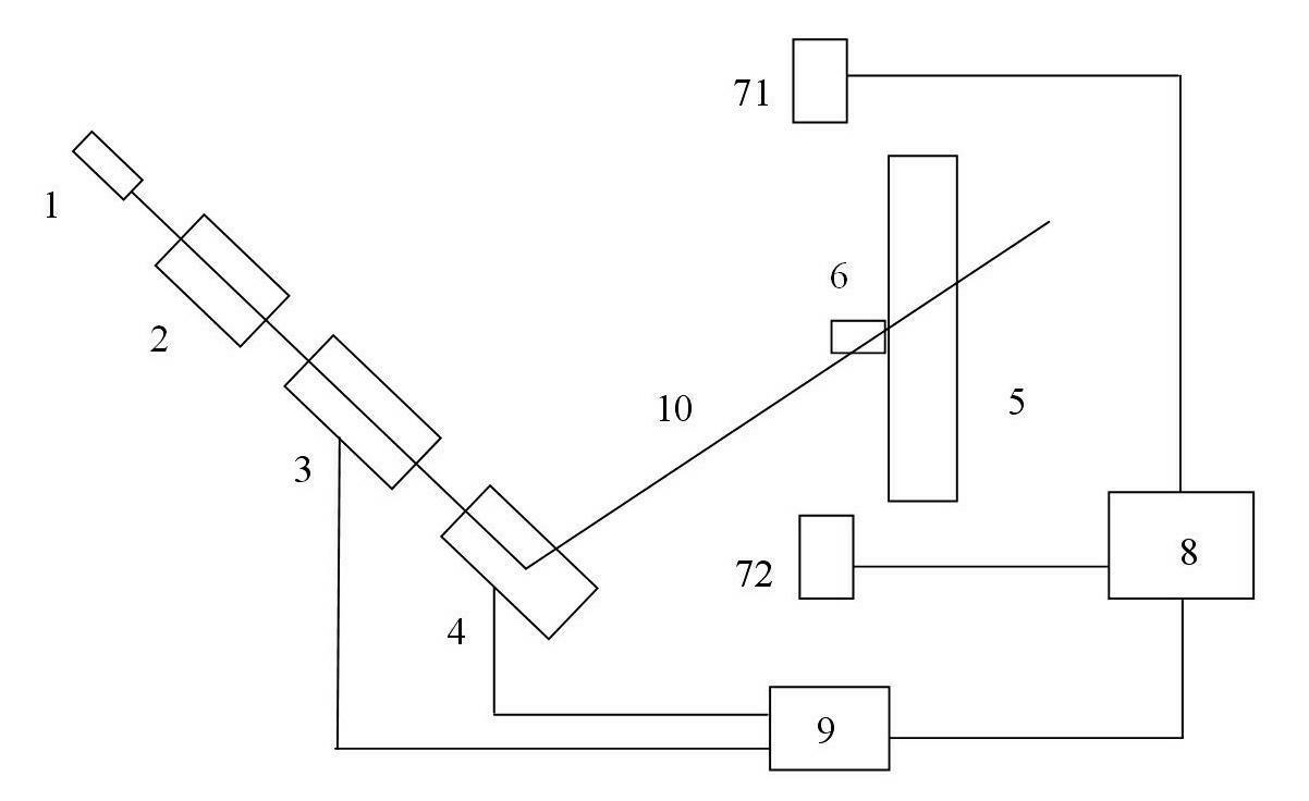
[0014] figure 1 It is a structural schematic diagram of an optical element surface defect detection system based on laser beam active scanning of the present invention. exist figure 1 Among them, an optical element surface defect detection system based on laser beam active scanning of the present invention includes a laser 1 , a beam expander 2 , a zoom lens 3 , a guide mirror 4 , a photoelectric probe, a computer 8 and a controller 9 . Among them, the laser 1, the beam expander 2, the zoom lens 3, and the guide mirror 4 are arranged in sequence; Fixed, the photoelectric probe is arranged outside the light-passing area of ​​the optical element 5; in the present embodiment, the photoelectric probe is set to two, namely the photoelectric probe I 71 and the photoelectric probe II 72, and the photoelectric probe I 71 and the photoelectric probe II 72 are respectively externally connected to the computer 8; control The controller 9 is connected with the computer 8, and the contro...

Embodiment 2

[0018] The basic structure of this embodiment is the same as that of Embodiment 1, and the difference is that the photoelectric probes are set to 12, and the 12 photoelectric probes are evenly distributed around the optical element 5, and the photoelectric probes detect scattered light from different angles, thereby improving The detection precision and accuracy of the equipment.

Embodiment 3

[0020] The basic structure of this embodiment is the same as that of Embodiment 1, except that the photoelectric probe can be a photomultiplier tube.


PUM


Abstract

The invention discloses an optical element surface defect detecting system based on active laser beam scanning. In the detecting system, relative movement is not performed between a to-be-monitored optical element and an optical maser, a guide lens, and a photoelectric probe; point-by-point scanning for the surface of the optical element can be realized only through the two-dimensional rotation of the guide lens; the position of the focal point of a laser beam can be changed in real time during scanning, so that the focal point can always fall on the surface of the optical element. The system can realize on-line monitoring of the optical element in a highlight irradiation environment, a high-vacuum environment and a confined space in a high-power solid laser device. The system disclosed by the invention has simple structure and wide application range, and is flexible to use.

Description

technical field [0001] The invention belongs to the field of optoelectronics. In particular, it relates to a detection system for surface defects of optical components based on active scanning of laser beams. It is especially suitable for on-line monitoring of surface defects of large-diameter optical components in high-power solid-state laser devices. Background technique [0002] At present, there are many methods that can detect surface defects. The commonly used methods include microscopic measurement, laser spectrum method, coherent filter imaging method, dark field imaging method, etc. developed in recent years. These detection methods can achieve higher detection accuracy. Accuracy, the measurement effect is better when used for offline detection. However, because the high-power solid-state laser device has a complex application environment, on the one hand, the interior of the optical transmission channel is mostly irradiated with strong light or high vacuum; In ...

Claims


Application Information

Patent Timeline
Patent Type & Authority Applications(China)
IPC IPC(8): G01N21/88G01N21/94
Inventor 程晓锋王洪彬徐旭叶亚云秦朗苗心向贺少勃吕海兵贺群马志强赵龙彪袁晓东郑万国
Owner LASER FUSION RES CENT CHINA ACAD OF ENG PHYSICS
Why Eureka
Try Eureka