Method for acquiring thickness change of photoresist and monitoring influence of photoresist thickness on graphic dimension

A technology for pattern size and thickness change, which is applied in microlithography exposure equipment, photolithography process exposure devices, semiconductor/solid-state device testing/measurement, etc., can solve the problem that the pattern size cannot be changed obviously, and the influence of pattern size cannot be found in time and other issues to achieve the effect of reducing requirements

Active Publication Date: 2014-04-09
SHANGHAI HUALI MICROELECTRONICS CORP
View PDF6 Cites 0 Cited by
  • Summary
  • Abstract
  • Description
  • Claims
  • Application Information

AI Technical Summary

Problems solved by technology

[0006] When using the swing curve to monitor the influence of the photoresist thickness on the pattern size, select the vertex a or the bottom point b as the monitoring point of the photoresist thickness, and measure the thickness by the film thickness measuring machine, but when the photoresist thickness changes, the pattern size will not change. Changes cannot be obvious, and the impact on the graphic size cannot be detected in time

Method used


Image

  • Method for acquiring thickness change of photoresist and monitoring influence of photoresist thickness on graphic dimension
  • Method for acquiring thickness change of photoresist and monitoring influence of photoresist thickness on graphic dimension
  • Method for acquiring thickness change of photoresist and monitoring influence of photoresist thickness on graphic dimension

Examples


no. 1 example

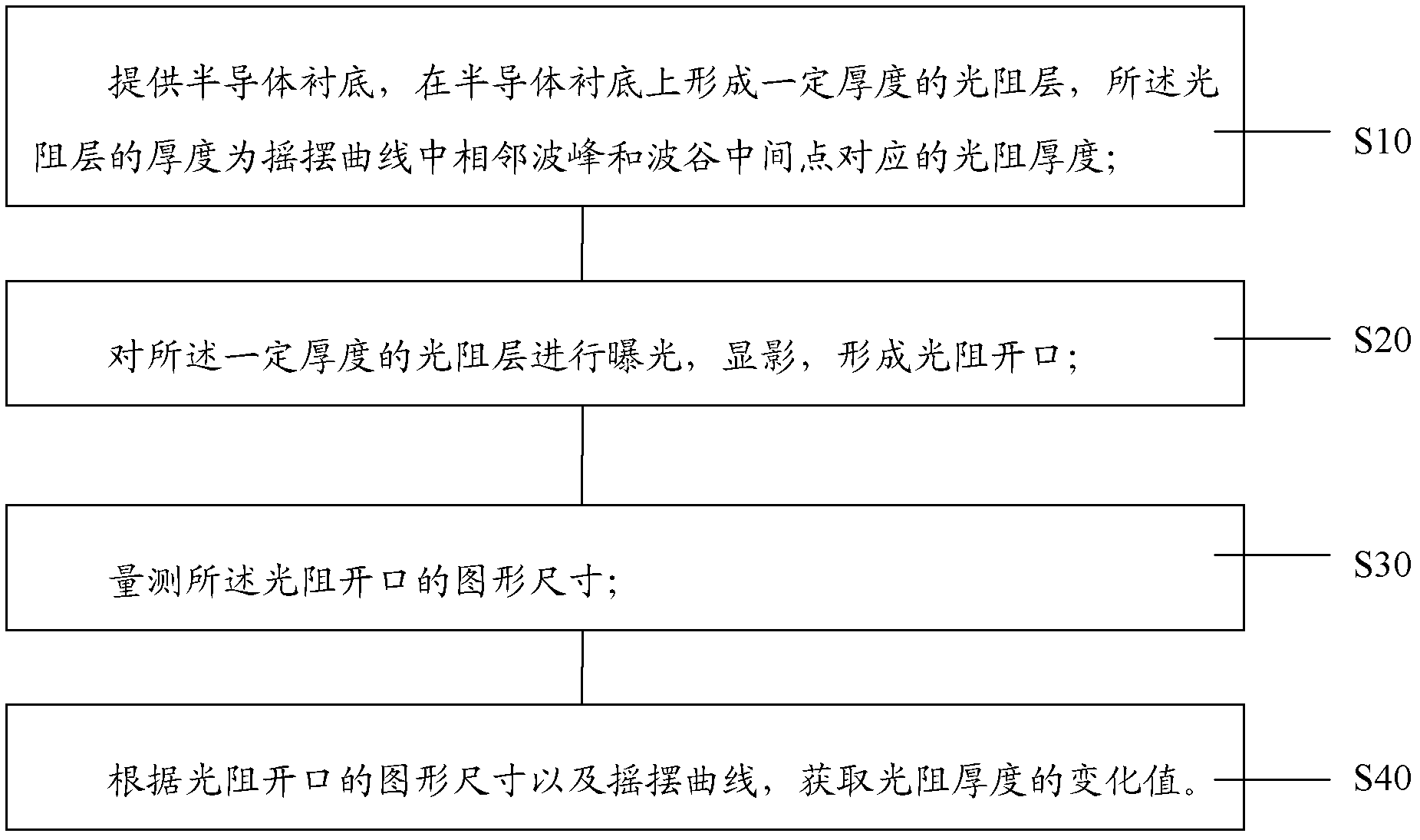
[0025] This embodiment provides a method to obtain the change of photoresist thickness, refer to the attached figure 2 shown, including the following steps:

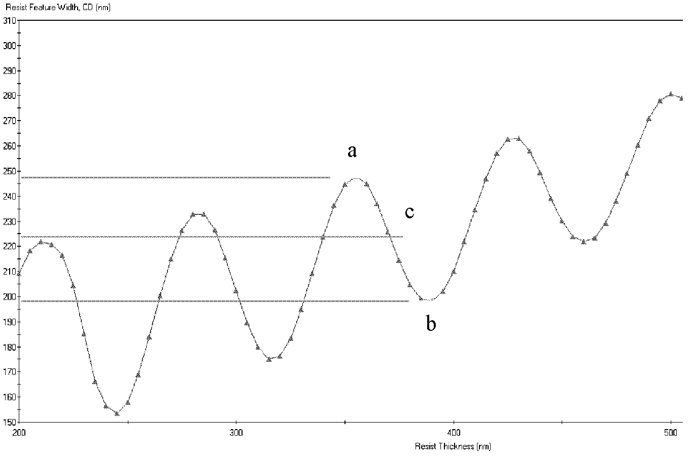
[0026] Step S10, providing a semiconductor substrate, forming a photoresist layer with a certain thickness on the semiconductor substrate, the thickness of the photoresist layer being the thickness of the photoresist corresponding to the middle point of the adjacent peak and trough in the rocking curve;

[0027] Wherein, the semiconductor substrate can be any material such as silicon, silicon germanium, silicon-on-insulator, etc., and the semiconductor substrate can be a blank substrate, or any semiconductor integrated circuit formed with semiconductor devices, interconnection structures, etc. Any intermediate structural state during the production process;

[0028] The photoresist layer of a certain thickness is formed by a conventional spin coating process, and the photoresist thickness selected in advance is the thi...

no. 2 example

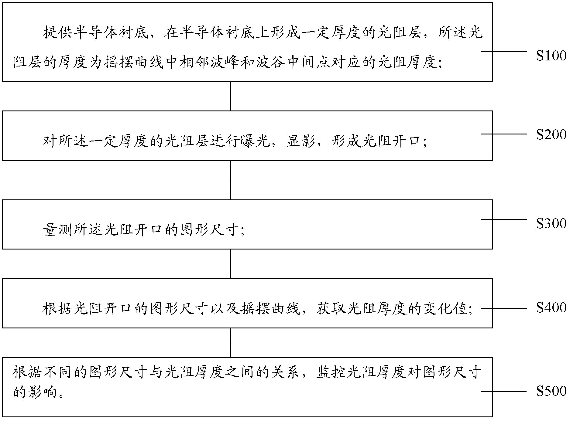
[0035] This embodiment provides a method for monitoring the influence of photoresist thickness on pattern size, refer to the attached image 3 shown, including the following steps:

[0036] Step S100, provide a semiconductor substrate, and form a photoresist layer with a certain thickness on the semiconductor substrate, the thickness of the photoresist layer is the thickness of the photoresist corresponding to the middle point of the adjacent peak and trough in the rocking curve;

[0037] Wherein, the semiconductor substrate can be any material such as silicon, silicon germanium, silicon-on-insulator, etc., and the semiconductor substrate can be a blank substrate, or any semiconductor integrated circuit formed with semiconductor devices, interconnection structures, etc. Any intermediate structural state during the production process;

[0038] The photoresist layer of a certain thickness is formed by a conventional spin coating process, and the photoresist thickness selected i...


PUM


Abstract

A method for acquiring thickness change of a photoresist comprises the following steps: providing a semiconductor substrate; forming a photoresist layer with a certain thickness on the semiconductor substrate; exposing the photoresist layer and developing to form a photoresist opening; measuring the graphic dimension of the photoresist opening; and acquiring the thickness change value of the photoresist according to the graphic dimension of the photoresist opening and a rocking curve, wherein the thickness of the photoresist layer corresponds to the intermediate point between the wave crest and the adjacent wave trough of the rocking curve. By selecting the photoresist thickness corresponding to the intermediate point between the wave crest and the adjacent wave trough of the rocking curve as the thickness monitor point, the method not only can acquire the thickness change of the photoresist, but also can monitor the influences of the photoresist thickness on the graphic dimension.

Description

technical field [0001] The invention relates to the field of semiconductor manufacturing, in particular to a method for obtaining the change of photoresist thickness and monitoring the influence of photoresist thickness on pattern size. Background technique [0002] The lithography process is a process of generating feature patterns with precise dimensions and correctly associated with other components at the correct position on the wafer surface according to the requirements of the circuit design. Photolithography is the most critical process step in all basic semiconductor manufacturing processes. Photolithography determines the minimum dimension that can be formed by all process steps in the device manufacturing process, that is, the critical dimension. [0003] The general photolithography process has to go through the processes of coating primer on the wafer surface, spin coating photoresist, soft baking, alignment, exposure, post-baking, developing, hard baking, etchi...

Claims


Application Information

Patent Timeline
Patent Type & Authority Patents(China)
IPC IPC(8): G03F7/20H01L21/66
Inventor 王剑
Owner SHANGHAI HUALI MICROELECTRONICS CORP
Why Eureka
Try Eureka