
Correlated three sampling circuits for CMOS (Complementary Metal-Oxide-Semiconductor Transistor) active pixel sensor

A technology of pixel sensor and sampling circuit, applied in the direction of TV, electrical components, color TV, etc., can solve the problem that the noise suppression effect deteriorates with the integration time, and achieve the effect of good noise suppression effect and simple circuit design.

Inactive Publication Date: 2012-06-20
SHANGHAI INST OF TECHNICAL PHYSICS - CHINESE ACAD OF SCI
View PDF4 Cites 8 Cited by
  • Summary
  • Abstract
  • Description
  • Claims
  • Application Information

AI Technical Summary

Problems solved by technology

[0005] The purpose of the present invention is to provide a row and column noise subtraction circuit to solve the problem that the noise suppression effect of the CDS method of the 3T structure CMOS-APS existing in the prior art becomes worse with the increase of the integration time

Method used


Image

  • Correlated three sampling circuits for CMOS (Complementary Metal-Oxide-Semiconductor Transistor) active pixel sensor
  • Correlated three sampling circuits for CMOS (Complementary Metal-Oxide-Semiconductor Transistor) active pixel sensor
  • Correlated three sampling circuits for CMOS (Complementary Metal-Oxide-Semiconductor Transistor) active pixel sensor

Examples


Embodiment Construction

[0013] Below in conjunction with accompanying drawing, the specific embodiment of the present invention is described in further detail:

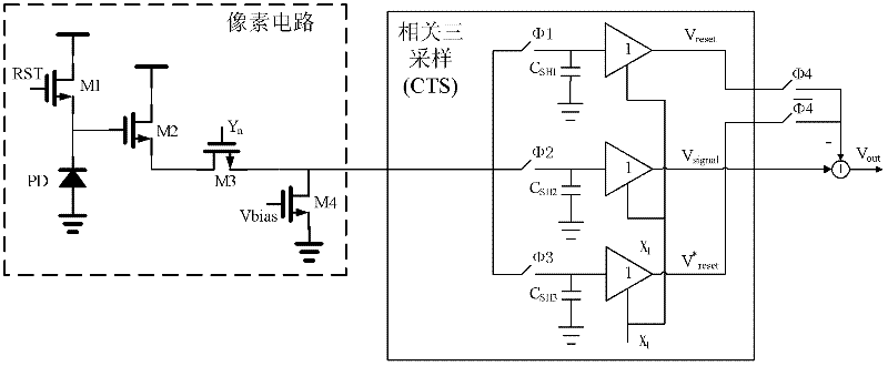
[0014] Such as figure 2 As shown, the relevant three-sampling circuit is composed of three independent sample-and-hold circuits. Each sample-and-hold circuit includes a switch, a capacitor, and an output Buffer. The switch is turned on and off by a periodic clock, which controls the charging and holding process of the column pixel bus to the capacitor. The turn-on time of the three switches is different, corresponding to the readout time of the "reset voltage", "signal voltage" and the "reset voltage" of the next frame. After charging the respective capacitors, they are turned off successively. . The output Buffer is also turned on and off controlled by the periodic clock. After the sampling capacitor is charged, the output Buffer is turned on by the clock control. These three voltage signals are output to the subsequent signal processin...


PUM


Abstract

The invention discloses correlated three sampling circuits for a CMOS (Complementary Metal-Oxide-Semiconductor Transistor) active pixel sensor, which relates to CMOS (Complementary Metal-Oxide-Semiconductor Transistor) active pixel sensor (APS) signal noise processing circuit design. Line degrees of the sensor adopt the correlated three sampling circuits, i.e. three line degree sampling hold circuits are sued for sampling and holding an output signal of a CMOS active pixel, so that two options for effectively inhibiting random noise in the pixel output signal under different working conditions, where one option is characterized in that: 'signal voltage' and 'reset voltage' of the pixel in the same frame are differentiated after being sampled and held, so that FPN (Fixed Pattern Noise) is eliminated and low frequency noise is inhibited; and the other option is characterized in that: 'signal voltage' of the pixel and 'reset voltage' of the next frame are differentiated after being sampled and held, so that FPN (Fixed Pattern Noise) is eliminated and low frequency noise is inhibited. The correlated three sampling circuits can provide different noise elimination schemes for different working conditions such as variation of integration time, and the noise can be better inhibited.

Description

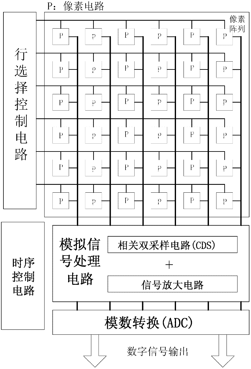
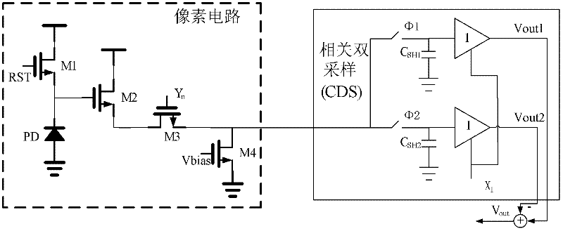
technical field [0001] The present invention relates to the design of CMOS active pixel sensor (APS) signal noise processing circuit, specifically refers to adopting a kind of correlation three-sampling circuit in the row and column level circuit of CMOS-APS, can use different sampling and holding schemes under different working conditions , suppressing the noise of CMOS-APS more effectively. Background technique [0002] So far, the solid-state image sensors used in the visible light band mainly include charge-coupled devices (CCDs) and complementary metal-oxide-semiconductor (CMOS) image sensors (CIS). Compared with CCD, CIS has been more and more widely used in various fields due to its advantages of low cost, low power consumption, and easy integration with other signal processing circuits. Although CIS also has its own shortcomings such as: the noise is generally larger than that of CCD, etc., these gaps will gradually become smaller with the advancement of technology ...

Claims


Application Information

Patent Timeline
IPC IPC(8): H04N5/374H04N5/378H04N5/357
Inventor 邓若汉陈永平陈世军余金金王洪彬
Owner SHANGHAI INST OF TECHNICAL PHYSICS - CHINESE ACAD OF SCI
Learn More