
Memory array structure with vertical transistor and forming method thereof

A technology of vertical transistors and memory arrays, applied in transistors, electric solid state devices, semiconductor devices, etc., can solve the problems of cumbersome process and unfavorable mass production, and achieve the effect of improving device performance, effective contact and avoiding influence

Active Publication Date: 2014-04-09
TSINGHUA UNIV
View PDF4 Cites 0 Cited by
  • Summary
  • Abstract
  • Description
  • Claims
  • Application Information

AI Technical Summary

Problems solved by technology

However, the process is cumbersome and is not conducive to mass production

Method used


Image

  • Memory array structure with vertical transistor and forming method thereof
  • Memory array structure with vertical transistor and forming method thereof
  • Memory array structure with vertical transistor and forming method thereof

Examples


Embodiment Construction

[0032] Embodiments of the present invention are described in detail below, examples of which are shown in the drawings, wherein the same or similar reference numerals designate the same or similar elements or elements having the same or similar functions throughout. The embodiments described below by referring to the figures are exemplary only for explaining the present invention and should not be construed as limiting the present invention.

[0033] In describing the present invention, it should be understood that the terms "center", "longitudinal", "transverse", "upper", "lower", "front", "rear", "left", "right", " The orientations or positional relationships indicated by "vertical", "horizontal", "top", "bottom", "inner", "outer", etc. are based on the orientation or positional relationships shown in the drawings, and are only for the convenience of describing the present invention and simplifying Describes, but does not indicate or imply that the device or element referred...


PUM


Abstract

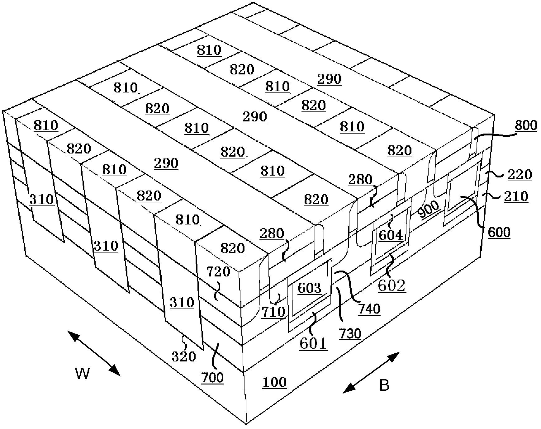
A memory array structure and a method for forming the same are provided. The memory array structure comprises: a substrate (100); a plurality of memory cells, each memory cell including a vertical transistor, of which a gate structure (603) is formed in a first trench (600) extending in a first direction; a plurality of word lines in the first direction, each word line formed in the first trench (600); a plurality of bit lines (700) in a second direction, each bit line (700) formed in lower sides of a semiconductor pillars (900); a plurality of body lines (280) in the first direction, each body line (280) having a first portion formed on the gate electrodes (603) and a second portion covering a part of a top surface of semiconductor pillar (900) for providing a substrate contact to vertical channel regions (740); and a plurality of data storage device contacts (820).

Description

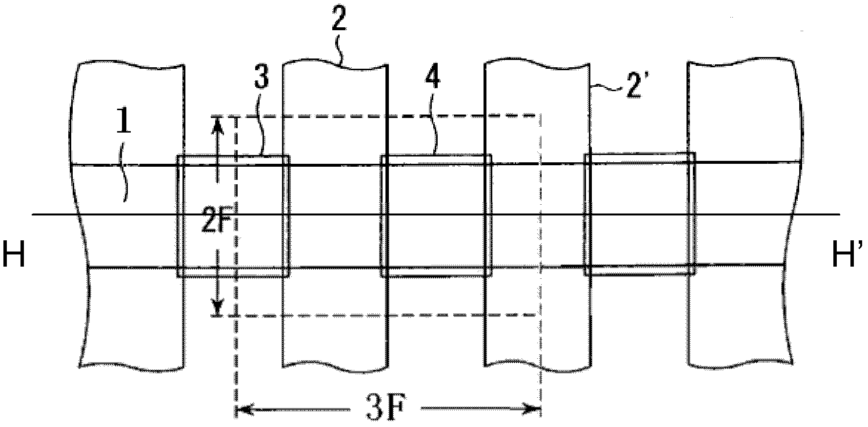
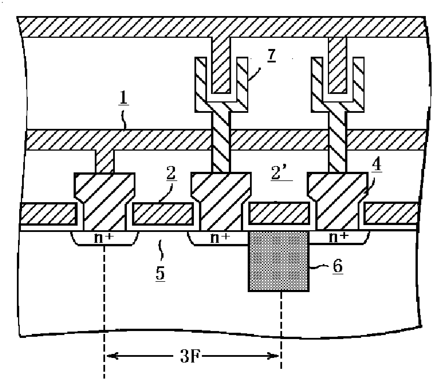
technical field [0001] The invention relates to the technical field of semiconductor design and manufacture, in particular to a storage array structure with vertical transistors and a forming method thereof. Background technique [0002] In the field of semiconductors, especially memory, methods to increase device integration include reducing device feature size and improving cell structure. However, as the feature size decreases, small-size transistors will produce serious short-channel effects; therefore, by improving the topology of the memory cell, reducing the area occupied by the memory cell under the same feature size is another way to increase the integration of the device. an efficient way. For example, in the field of DRAM (Dynamic Random Access Memory, dynamic random access memory), the existing mainstream process uses 6F2 cells instead of 8F2 cells to significantly increase the integration level of DRAM. figure 1 is a top view of the 6F2 DRAM memory cell array,...

Claims


Application Information

Patent Timeline
Patent Type & Authority Patents(China)
IPC IPC(8): H01L27/108H01L21/8242H10B12/00
CPCH01L27/10876H01L27/10885H01L27/10823H10B12/34H10B12/053H10B12/482
Inventor 潘立阳麻昊志
Owner TSINGHUA UNIV
Learn More