Method for fabricating semiconductor device with vertical channel transistor

a vertical channel transistor and semiconductor technology, applied in the direction of semiconductor devices, basic electric elements, electrical appliances, etc., can solve the problems of difficult to meet the requirements of a device area and deterioration of device characteristics, so as to prevent damage to a pillar and minimize the loss of hard mask patterns and spacers

Active Publication Date: 2010-03-02
SK HYNIX INC
View PDF7 Cites 14 Cited by
  • Summary
  • Abstract
  • Description
  • Claims
  • Application Information

AI Technical Summary

Benefits of technology

[0009]In the vertical channel transistor where a channel is formed vertically with respect to a surface of the substrate, a channel length can be increased without being limited to a device area, thus preventing the short channel effect. However, there is a limitation in a process for forming the word line 102, resulting in a device failure. Hereinafter, one method for fabricating the vertical channel transistor in the substrate and the limitation thereof will be described in detail with reference to FIGS. 2A to 2C.
[0012]An oxide layer 204 is formed over a resultant structure, and then planarized through chemical mechanical polishing (CMP) process until the first hard mask pattern 201 is exposed. After a second hard mask 205 is formed on the planarized resultant structure, a photoresist pattern 207 is formed over the hard mask 205 for the purpose of forming a word line. An anti-reflective layer 206 may be formed under the photoresist pattern 207 to prevent reflection during photo exposure process.
[0016]Hence, it is required to develop a new, more preferred fabrication technique capable of preventing the pillar P from being attacked by minimizing the losses of the hard mask pattern 201 and the spacer 202 even though the misalignment occurs due to an overlay error of a mask.
[0017]At least one preferred embodiment of the present invention is therefore directed to providing a method for fabricating a semiconductor device with a vertical channel transistor, which can minimize losses of a hard mask pattern and a spacer to prevent a pillar from being damaged, by dividing a process of forming a trench for a word line into two sub processes and performing a process of forming a buffer layer between the two sub processes.

Problems solved by technology

As the integration degree of a semiconductor device increases, a channel length of a transistor is gradually reduced, causing device characteristics to be deteriorated due to a short channel effect.
Therefore, it is difficult to meet the requirement for a device area despite the scaling-down of a channel length in a typical planar transistor structure where a gate electrode is formed over a substrate and junction regions are formed at both sides of the gate electrode.

Method used


Image

  • Method for fabricating semiconductor device with vertical channel transistor
  • Method for fabricating semiconductor device with vertical channel transistor
  • Method for fabricating semiconductor device with vertical channel transistor

Examples


Embodiment Construction

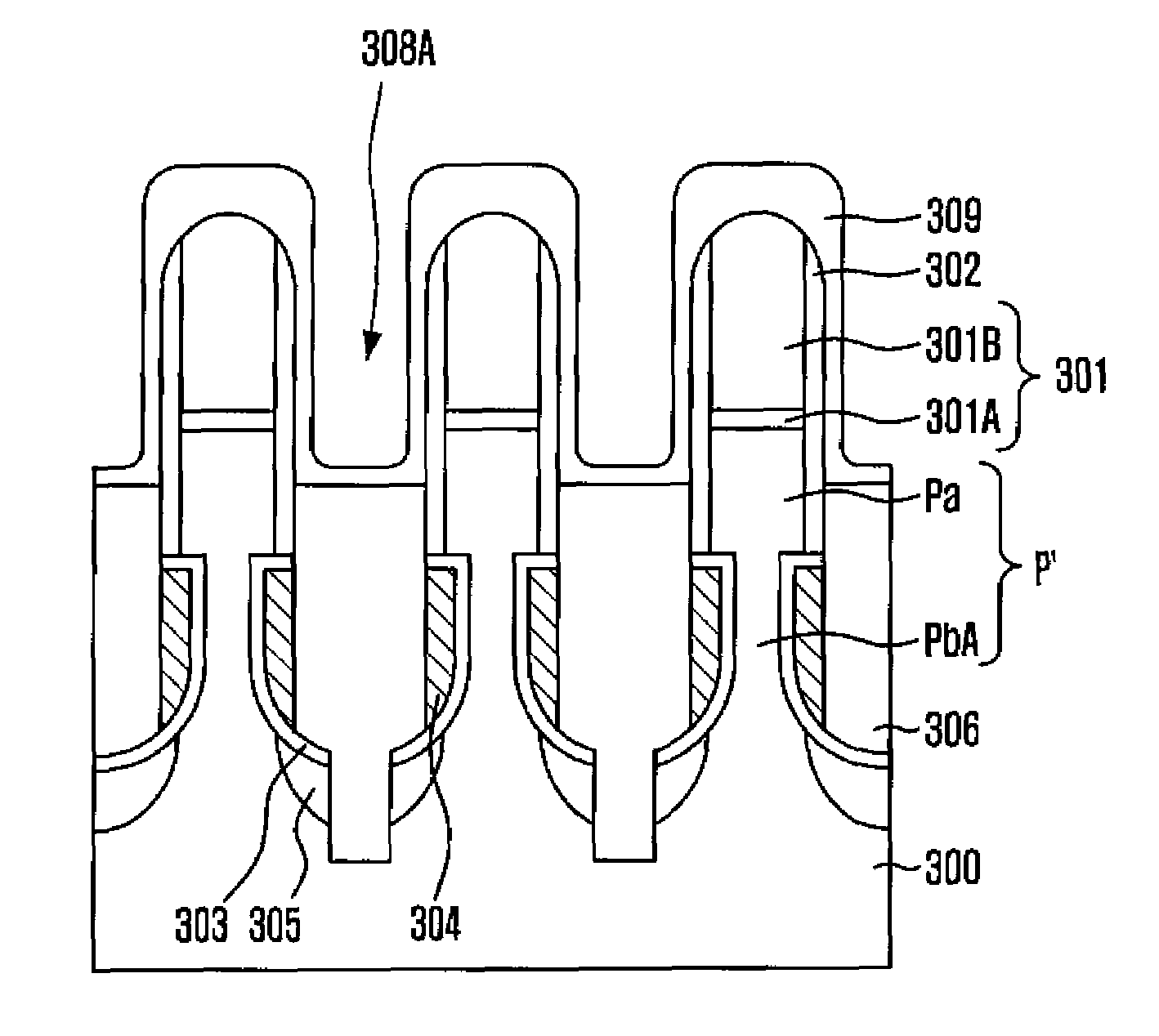
[0022]FIGS. 3A to 3J illustrate a method for fabricating a vertical channel transistor in a semiconductor device in accordance with an embodiment of the present invention. In particular, FIGS. 3A to 3J illustrate cross-sectional views taken along line Y-Y″ of FIG. 1, i.e., a second direction.

[0023]Referring to FIG. 3A, a plurality of first hard mask patterns 301, which are arranged in a first direction and a second direction crossing the first direction, are formed over a substrate 300. Preferably, the first hard mask pattern 301 has a multi-layered structure of an oxide layer 301A and a nitride layer 301B. The substrate 300 is etched to a predetermined depth using the first hard mask pattern 301 as an etch barrier to thereby form an upper pillar Pa.

[0024]Referring to FIG. 3B, a spacer 302 is formed on sidewalls of the first hard mask pattern 301 and the upper pillar Pa. Preferably, the spacer 302 is formed of a nitride. The exposed substrate 300 is etched to a predetermined depth u...


PUM


Abstract

A method for fabricating a semiconductor memory device with a vertical channel transistor includes forming a plurality of pillars each having a hard mask pattern thereon over a substrate, each of the plurality of pillars comprising an upper pillar and a lower pillar; forming a surround type gate electrode surrounding the lower pillar; forming an insulation layer filling a space between the pillars; forming a preliminary trench by primarily etching the insulation layer using a mask pattern for a word line until a portion of the upper pillar is exposed; forming a buffer layer over a resultant structure including the preliminary trench except on a bottom of the preliminary trench; and forming a trench for a word line by secondarily etching the insulation layer until the surround type gate electrode is exposed.

Description

CROSS-REFERENCE TO RELATED APPLICATIONS[0001]The present invention claims priority of Korean patent application number 2007-0136437, filed on Dec. 24, 2007, which is incorporated by reference in its entirety.BACKGROUND OF THE INVENTION[0002]The present invention relates to semiconductor device fabrication technology, and more particularly, to a method for fabricating a semiconductor device with a vertical channel transistor.[0003]As the integration degree of a semiconductor device increases, a channel length of a transistor is gradually reduced, causing device characteristics to be deteriorated due to a short channel effect. To avoid the short channel effect, there have been proposed various methods of reducing a depth of a junction region or relatively increasing a channel length by recessing a channel region of a transistor.[0004]However, there is an increasing demand for a smaller-sized transistor as the integration density of a semiconductor memory device such as a dynamic rando...

Claims


Application Information

Patent Timeline
Patent Type & Authority Patents(United States)
IPC IPC(8): H01L29/732
CPCH01L27/10876H01L29/66666H01L29/7827H10B12/053H10B12/395H10B12/0383
Inventor CHO, SANG-HOON
Owner SK HYNIX INC
Why Eureka
Try Eureka