Method of fabricating fin field effect transistor using isotropic etching technique

a technology of isotropic etching and fin field effect, which is applied in the direction of transistors, semiconductor devices, electrical equipment, etc., can solve the problems of deterioration of charge retention characteristics, leakage current increase between channel regions, source and drain regions, and reduce current driving capability, etc., to achieve short channel effect and high integration

Active Publication Date: 2006-12-26
SAMSUNG ELECTRONICS CO LTD
View PDF10 Cites 14 Cited by
  • Summary
  • Abstract
  • Description
  • Claims
  • Application Information

AI Technical Summary

Benefits of technology

[0011]Embodiments of the invention provide methods of fabricating FinFETs by optimizing a method for forming the fin so that a short channel effect is prevented and high integration is achieved.
[0014]In yet another embodiment, the hard mask pattern may further include a pad oxide layer. The pad oxide layer is employed to reduce the stress between the lower hard mask pattern and the semiconductor substrate.
[0018]In another embodiment, the invention is directed to a method of fabricating a FinFET. This method includes forming a hard mask pattern on a semiconductor substrate. The semiconductor substrate is etched, using the hard mask pattern as an etching mask, to form a trench for defining an active region. An isolation layer is then formed to fill the trench and cover sidewalls of the hard mask pattern. A photoresist pattern is then formed to have a groove extending across the hard mask pattern. The isolation layer is etched, using the photoresist pattern and the hard mask pattern, as an etching mask to expose both sidewalls of the active region, and the photoresist pattern is removed. The sidewalls of the exposed active region are then recessed using, for example, the isotropic etching technique to form a fin, and the hard mask pattern is removed to expose an upper surface of the fin. A gate electrode is then formed to cover the exposed upper surface and sidewalls of the fin. In this case, the gate electrode is insulated from the fin. According to another embodiment of the present invention, the active region may be recessed, using the isotropic etching technique, to form the fin and simplify the process.

Problems solved by technology

However, when the channel region is highly doped, channel resistance increases to thereby reduce current driving capability.
As a result, leakage current increases between the channel region, and the source and drain regions.
In particular, when a capacitor for storing charges, as in a DRAM cell, is connected to the source or drain region, the increase of the leakage current leads to deterioration of the charge retention characteristics.
However, there exists a limitation to form the hard mask pattern having a narrow width by patterning the hard mask, using the photolithography-etching technique.

Method used


Image

  • Method of fabricating fin field effect transistor using isotropic etching technique
  • Method of fabricating fin field effect transistor using isotropic etching technique
  • Method of fabricating fin field effect transistor using isotropic etching technique

Examples


Embodiment Construction

[0027]The present invention will now be described more fully hereinafter with reference to the accompanying drawings, in which exemplary embodiments of the invention are shown. In the drawings, the thickness of the layers and regions are exaggerated for clarity.

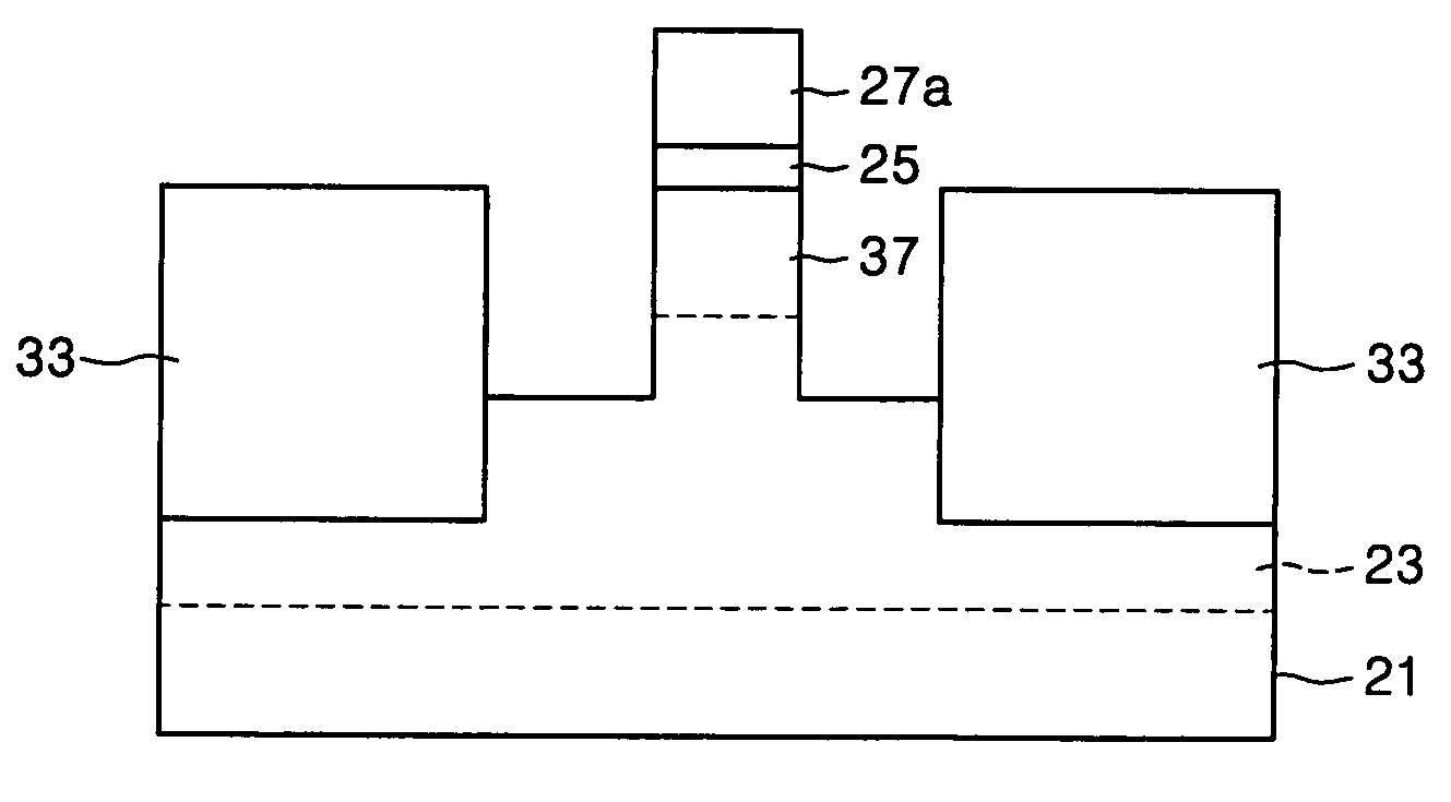
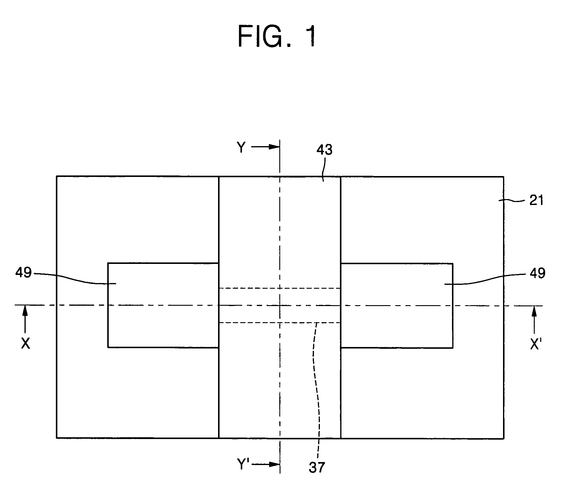
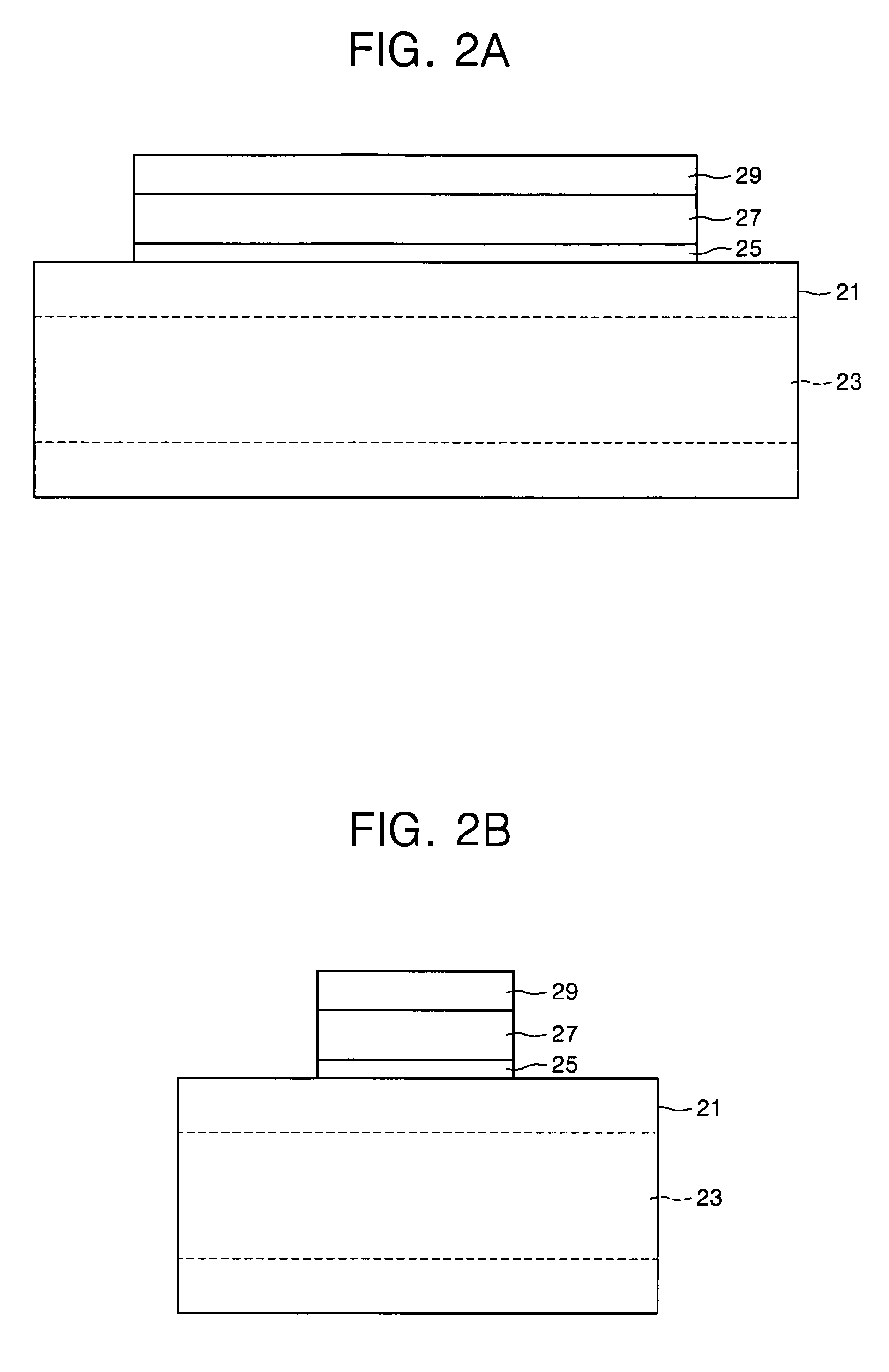
[0028]FIG. 1 is a layout illustrating a method of fabricating the FinFET in accordance with embodiments of the present invention, and FIG. 2A to FIG. 9B are cross-sectional views, taken along lines X–X′ and Y–Y′ of FIG. 1, illustrating a method of fabricating the FinFET in accordance with exemplary embodiments of the present invention. In FIG. 2A to FIG. 9B, alphabetical reference “A” indicates cross-sectional views taken along line X–X′ of FIG. 1, and “B” indicates cross-sectional views taken along line Y–Y′ of FIG. 1.

[0029]Referring to FIGS. 1, 2A, and 2B, a hard mask pattern is formed on a semiconductor substrate 21. The semiconductor substrate 21 may be a P type silicon substrate. In this case, a channel stopping region 2...


PUM


Abstract

Methods of fabricating a fin field effect transistor (FinFET) are disclosed. Embodiments of the invention provide methods of fabricating FinFETs by optimizing a method for forming the fin so that a short channel effect is prevented and high integration is achieved. Accordingly, the fin which has a difficulty in its formation using the current photolithography-etching technique may be readily formed.

Description

CROSS-REFERENCE TO RELATED APPLICATION[0001]This application claims the benefit of Korean Patent Application No. 2004-18122, filed Mar. 17, 2004, the contents of which are hereby incorporated herein by reference in their entirety.BACKGROUND OF THE INVENTION[0002]1. Field of the Invention[0003]The present invention relates to a method of fabricating a semiconductor device and, more particularly, to a method of fabricating a fin field effect transistor (FinFET) using an isotropic etching technique.[0004]2. Description of Related Art[0005]Semiconductor devices widely employ discrete devices such as Metal Oxide Semiconductor (MOS) transistors as switching devices. As integration of the semiconductor device increases, the sizes of MOS transistors are scaled down. As a result, the channel length of the MOS transistor is reduced so that a short channel effect may easily occur.[0006]In general, methods for highly doping channel ions within a channel region are used to prevent a threshold vo...

Claims


Application Information

Patent Timeline
Patent Type & Authority Patents(United States)
IPC IPC(8): H01L21/336H01L21/331H01L21/8234H01L29/78H01L29/786
CPCH01L29/66818H01L29/7851H01L29/42312H01L29/66348H01L29/7813H01L29/785
Inventor SEO, HYEOUNG-WONYANG, WOUN-SUCKSONG, DU-HEONYOON, JAE-MAN
Owner SAMSUNG ELECTRONICS CO LTD
Why Eureka
Try Eureka