Field-induced tunneling enhanced HEMT (high electron mobility transistor) device

An enhanced, tunneling technology, applied in semiconductor devices, electrical components, circuits, etc., can solve problems such as gate control weakening, reducing device transconductance, injection damage, etc., to achieve the effect of improving control and withstand voltage

Inactive Publication Date: 2013-01-16
UNIV OF ELECTRONICS SCI & TECH OF CHINA
View PDF3 Cites 13 Cited by
  • Summary
  • Abstract
  • Description
  • Claims
  • Application Information

AI Technical Summary

Problems solved by technology

Among them, reducing the Al composition or growing a thin barrier layer reduces the 2DEG concentration in the channel and increases the parasitic resistance and on-state resistance of AlGaN/GaN HEMTs, so the Al composition and barrier layer thickness can only be limited in a limited range. Inner reduction; grow InGaN capping layer or p-GaN capping layer to make enhanced HEMT, the capping layer weakens the control of the gate on the channel, reduces the transconductance of the device, which is no

Method used


Image

  • Field-induced tunneling enhanced HEMT (high electron mobility transistor) device
  • Field-induced tunneling enhanced HEMT (high electron mobility transistor) device
  • Field-induced tunneling enhanced HEMT (high electron mobility transistor) device

Examples


Embodiment Construction

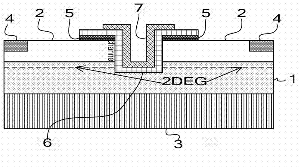
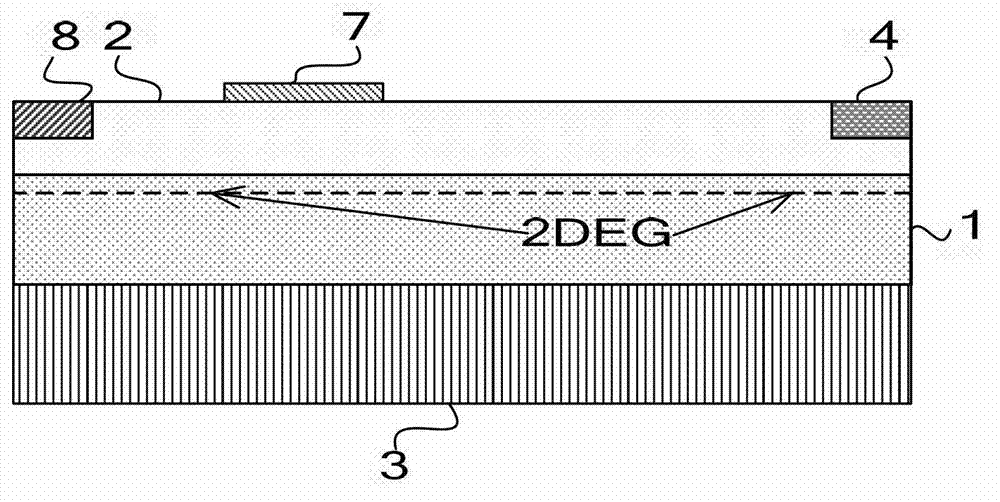
[0032] A field-induced tunneling enhanced HMET device, its structure is as follows figure 1 As shown, it includes a silicon substrate 3, a GaN heterojunction formed by GaN layer 1 and MGaN layer 2, a gate structure, a source structure and a drain structure, wherein M is a group III element other than Ga; the drain The electrode structure is formed by the metal drain electrode 4 located on the upper layer of the GaN heterojunction, that is, the surface of the AlGaN layer 2, and forms an ohmic contact with the surface of the MGaN layer 2; the gate structure is a grooved insulated gate structure, including an etched A groove in a GaN heterojunction, the inner wall of the groove has an insulating gate dielectric 6 in contact with the GaN layer 1 and the MGaN layer 2, and the inside of the groove is filled with metal to form a metal gate electrode 7; the source structure is formed by a structure close to the gate And away from the drain structure, a metal source electrode 5 forming...


PUM


Abstract

The invention belongs to the technical field of semiconductor devices, and particularly relates to a field-induced tunneling enhanced HEMT (high electron mobility transistor) device. The field-induced tunneling enhanced HEMT device is different from conventional AlGaN/GaN HEMT devices in that metal sources are in Schottky barrier contact instead of ohm contact in conventional structures; and metal gates are not positioned between the sources and drains but form insulating gate electrodes at the edges, away from the drains, of the sources through etching grooves. Field-control conductive channels are realized by means of the insulating layer and groove technology, field control of the field-control conductive channels is realized by voltage applied to the groove gate electrodes, and electrons subjected to band bending can directly tunnel barriers to be accumulated below the channels in gate modulation when forward voltage is applied to the gate electrodes, so that normally closed channels are realized, and frequency characteristics of the device can be promoted without affecting reverse voltage withstand capability of the device. Meanwhile, the preparation process of the device is compatible to traditional processes, and thereby solid foundation is established for the GaN power integration technology.

Description

technical field [0001] The invention belongs to the technical field of semiconductor devices and relates to a high electron mobility transistor (HEMT). Background technique [0002] Gallium nitride (GaN) is one of the representatives of the third generation of wide bandgap semiconductors, with excellent characteristics: high critical breakdown electric field (~3.5×10 6 V / cm), high electron mobility (~2000cm 2 / V·s), high two-dimensional electron gas (2DEG) concentration (~10 13 cm -2 ), high temperature working ability. High electron mobility transistors (HEMTs) based on AlGaN / GaN heterojunctions (or heterojunction field effect transistors HFETs, modulated doped field effect transistors MODFETs, hereinafter collectively referred to as HEMT devices) have been widely used in the semiconductor field. This type of device has the characteristics of high reverse blocking voltage, low forward conduction resistance, and high operating frequency, so it can meet the system's requi...

Claims


Application Information

Patent Timeline
IPC IPC(8): H01L29/06H01L29/423H01L29/778
Inventor 陈万军张竞尉中杰魏进张波
Owner UNIV OF ELECTRONICS SCI & TECH OF CHINA
Why Eureka
Try Eureka