Reverse blocking type IGBT and manufacturing method therefor

A reverse-resistance type and N-type technology, applied in the field of power semiconductor devices, can solve the problems of increasing the saturation current density of the device, increasing the capacitance of the device gate, and reducing the switching speed of the device, so as to increase the reverse breakdown voltage and reduce the gate voltage. Capacitance, enhance the effect of reliability

Active Publication Date: 2018-03-13
UNIV OF ELECTRONICS SCI & TECH OF CHINA
View PDF5 Cites 18 Cited by
  • Summary
  • Abstract
  • Description
  • Claims
  • Application Information

AI Technical Summary

Problems solved by technology

[0008] On the one hand, the implementation of method (2) will increase the gate capacitance of the device, resulting in a decrease in the switching speed of the device and an increase in switching loss, which will affect the compromise between the conduction voltage drop and switching loss of the device. On the other hand, the large channel Density will also increase the saturation current density of the device, deteriorating the short-circuit safe operating area of ​​the device
[0009] In addition, the gate oxide layer in the trench gate structure of the IGBT device is formed in the trench by one-time thermal oxidation. In order to ensure a certain threshold voltage, the thickness of the entire gate oxide layer is required to be small. However, the capacitance of the MOS and the oxide layer The thickness is inversely proportional to the thickness, which makes the thin gate oxide layer thickness in traditional IGBT devices will also significantly increase the gate capacitance of the device; at the same time, the electric field concentration effect at the bottom of the trench will cause the breakdown voltage of the device to decrease, resulting in poor reliability of the device ; Moreover, IGBT still has the disadvantage of poor reverse blocking ability of FS-IGBT structure, so it is difficult to be directly applied to applications that require IGBT to have reverse blocking ability

Method used


Image

  • Reverse blocking type IGBT and manufacturing method therefor
  • Reverse blocking type IGBT and manufacturing method therefor
  • Reverse blocking type IGBT and manufacturing method therefor

Examples


Embodiment 1

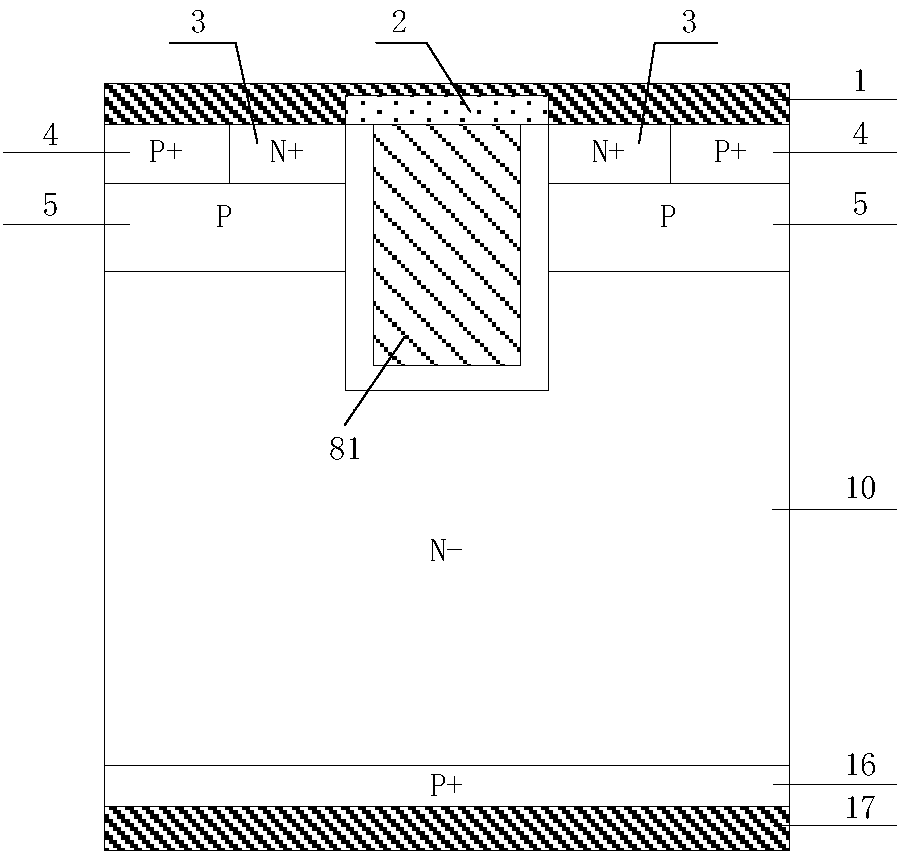
[0086] This embodiment provides a reverse resistance type IGBT, the cell structure of which is as follows image 3 As shown, it includes a collector metal 17, a P-type collector region 16, an N-type electric field stop layer 15, an N-type drift region 10 and an emitter metal 1 stacked sequentially from bottom to top; it is characterized in that: the N-type The drift region 10 has an N+ emitter region 3, a P+ emitter region 4, a P-type base region 5, an N-type charge storage layer 6 and a trench gate structure; the top layer of the N-type drift region 10 also has a first floating P Type body region 9, the first floating P-type body region 9 is located on one side of the trench gate structure and connected to it, N+ emitter region 3, P+ emitter region 4, P-type base region 5, and N-type charge storage layer 6 are located The other side of the trench gate structure; the N+ emitter region 3 and the P+ emitter region 4 are in contact with each other and are located side by side und...

Embodiment 2

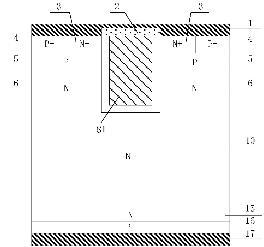
[0088] This embodiment provides a reverse resistance type IGBT, the cell structure of which is as follows Figure 4 As shown, it includes: a collector metal 17, a P-type collector region 16, an N-type electric field stop layer 15, an N-type drift region 10 and an emitter metal 1 stacked sequentially from bottom to top; it is characterized in that: the N Type drift region 10 has N+ emitter region 3, P+ emitter region 4, P-type base region 5, N-type charge storage layer 6, split trench gate structure and trench collector structure; N+ emitter region 3 and P+ emitter region 4 They are in contact with each other and are located side by side under the emitter metal 1 and connected to the emitter metal 1; the P-type base region 5 is located under the N+ emitter region 3 and the P+ emitter region 4 and is connected to the two, and the N-type charge storage layer 6 is located on the P between the N-type base region 5 and the N-type drift region 10; the split trench gate structure incl...

Embodiment 3

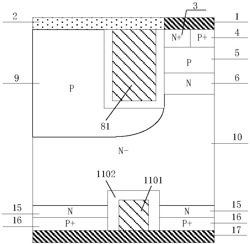
[0090] This embodiment provides a reverse resistance type IGBT, the cell structure of which is as follows Figure 5 As shown, the structure of this embodiment is the same as that of Embodiment 1 except that a P-type layer 12 connected to the trench bottom of the trench collector structure is provided in this embodiment. This embodiment further improves the reverse breakdown voltage of the device.


PUM


Abstract

The invention discloses a reverse blocking type IGBT and a manufacturing method therefor, and belongs to the technical field of a power semiconductor device. By introducing a floating P type body region on one side of a trench gate and introducing a trench collector structure in a collector region and a field stop layer, the positive breakdown voltage of a device is improved without influencing the threshold voltage and switch-on of an IGBT device; the gate-collector capacitance is lowered, and adverse influence caused by a Miller effect can be relieved; the overall gate capacitance is lowered, the switching speed of the device is improved, the switching loss of the device is lowered, and the compromising relation between forward switch-on voltage drop and switch-off loss of the conventional CSTBT device is improved; the problems of current, voltage oscillation and EMI in the device starting dynamic process can be avoided, and device reliability is improved; the current carrier enhancement effect at the emitter end of the device is improved, the current carrier concentration distribution in a drift region can be improved, and compromising between forward switch-on voltage drop andswitch-off loss can be further improved; and the reverse breakdown voltage of the device is improved, and high forward characteristic of the device is ensured while excellent reverse blocking performance is obtained.

Description

technical field [0001] The invention belongs to the technical field of power semiconductor devices, and relates to an insulated gate bipolar transistor (IGBT), in particular to a reverse resistance IGBT and a manufacturing method thereof. Background technique [0002] An insulated gate bipolar transistor (IGBT) is a power semiconductor device composed of a MOS field effect transistor (MOSFET) and a bipolar junction transistor (BJT), which can be equivalent to a MOSFET driven by a bipolar junction transistor. IGBT combines the working mechanism of MOSFET structure and bipolar junction transistor. It not only has the advantages of easy driving of MOSFET, low input impedance and fast switching speed, but also has the advantages of high on-state current density, low conduction voltage, low loss and stability of power transistor. The advantages of good performance make it significantly improve the performance of power electronic systems in applications. At present, IGBT has beco...

Claims


Application Information

Patent Timeline
Patent Type & Authority Applications(China)
IPC IPC(8): H01L29/739H01L21/331H01L29/06
CPCH01L29/0603H01L29/0684H01L29/66325H01L29/7393
Inventor 张金平赵倩刘竞秀李泽宏任敏张波
Owner UNIV OF ELECTRONICS SCI & TECH OF CHINA
Why Eureka
Try Eureka