Semiconductor device, finfet transistor and fabrication method thereof

a technology of semiconductor devices and fins, applied in semiconductor devices, semiconductor/solid-state device details, electrical apparatus, etc., can solve the problems of severe leakage current problems, inability to match the performance requirements of ic devices, and weak control ability of planar cmos transistors to channel regions, etc., to achieve the effect of increasing the heat dissipation efficiency of semiconductor devices

Active Publication Date: 2016-12-01
SEMICON MFG INT (SHANGHAI) CORP
View PDF2 Cites 13 Cited by
  • Summary
  • Abstract
  • Description
  • Claims
  • Application Information

AI Technical Summary

Benefits of technology

[0008]One aspect of the present disclosure includes a method for fabricating a semiconductor device. The method includes providing a semiconductor substrate having a surface; forming at least one fin over the surface of the semiconductor substrate; forming a mask layer on side surfaces of the fin; forming insulation layer trenches in the semiconductor substrate by etching the semiconductor substrate using the mask layer as an etching mask; forming silicon oxide layers on the side surfaces of the insulation trenches under the fins; forming first nitrogen-doped silicon oxide layers by doping nitrogen into the silicon oxide layers; and filling the insulation layer trenches with nitrogen-doped silicon oxide to form second nitrogen-doped silicon oxide layers. The first nitrogen-doped silicon oxide layers and the second nitrogen-doped silicon oxide layers form an insulation layer under the fin to inhibit a short channel effect and increase a heat dissipation efficiency of the semiconductor device.
[0010]Another aspect of the present disclosure includes a fin field-effect transistor. The fin field-effect transistor includes a semiconductor substrate; an insulation layer configured for inhibiting a short channel effect and increasing a heat dissipation efficiency of the fin field-effect transistor formed over the semiconductor substrate; at least one fin formed over the insulation layer; a gate structure crossing over at least one fin and covering side and top surfaces of the fin formed over the semiconductor substrate; and a source formed in the fin at one side of the gate structure and a drain formed in the fin the other side of the gate structure.

Problems solved by technology

However, with the continuous shrinking of the CD, the conventional planar MOS transistors are unable to match the performance requirements of IC devices.
For example, the control ability of the planar CMOS transistors to their channel regions has become relatively weak; and a severe leakage current issue may occur.
Therefore, the existing FinFETs may be unable to match the development of the ICs.

Method used


Image

  • Semiconductor device, finfet transistor and fabrication method thereof
  • Semiconductor device, finfet transistor and fabrication method thereof
  • Semiconductor device, finfet transistor and fabrication method thereof

Examples


Embodiment Construction

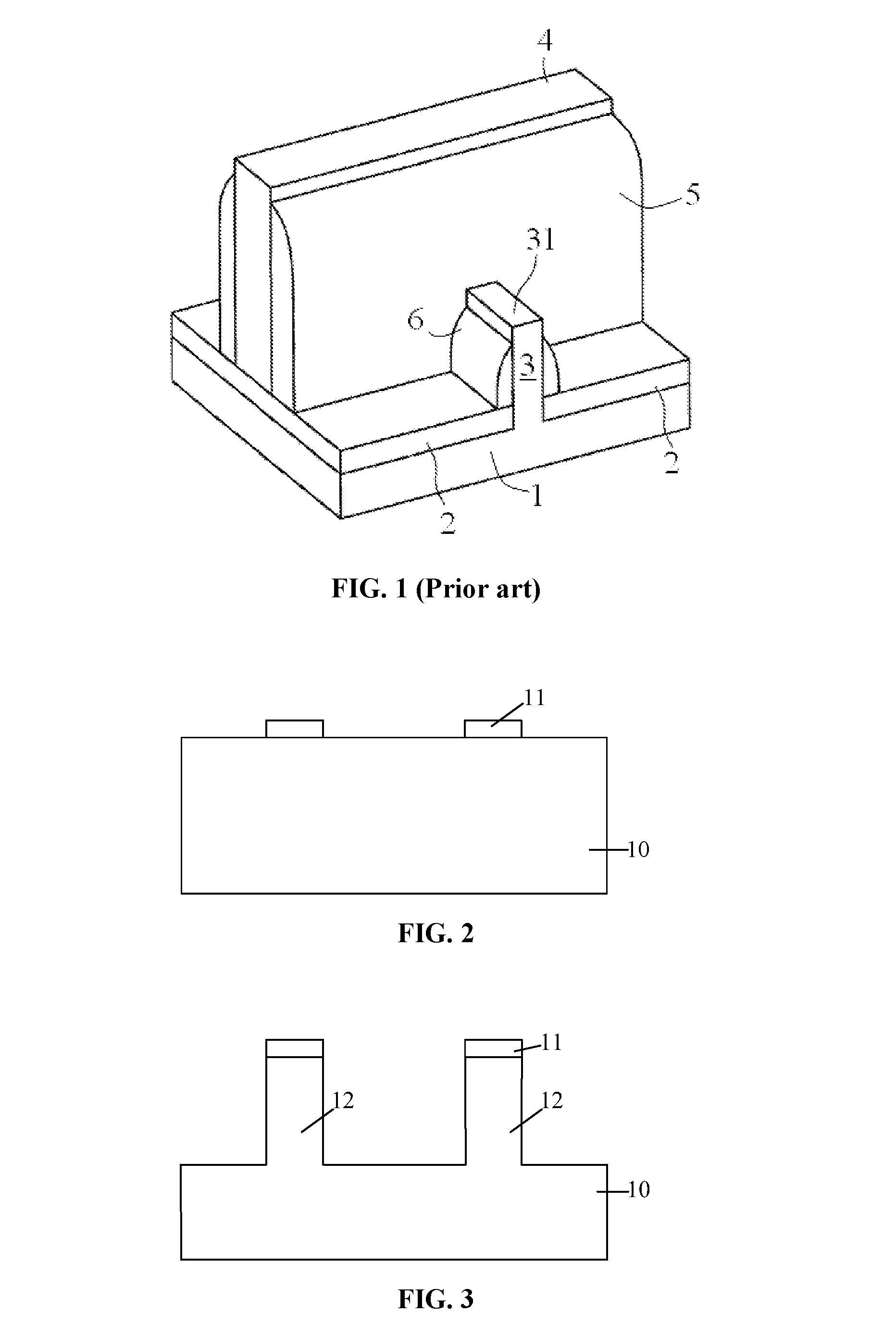
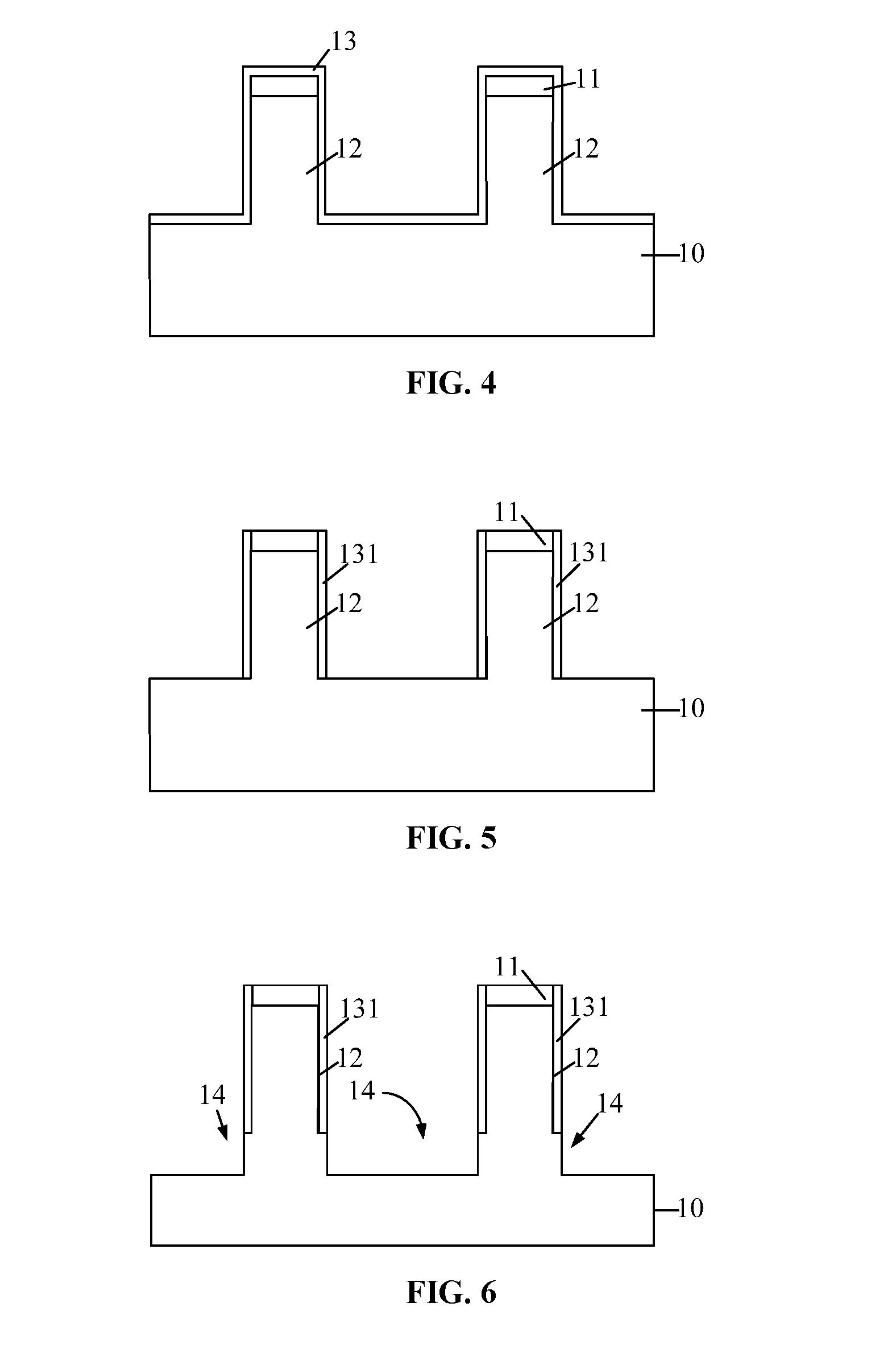
[0016]Reference will now be made in detail to exemplary embodiments of the invention, which are illustrated in the accompanying drawings. Wherever possible, the same reference numbers will be used throughout the drawings to refer to the same or like parts.

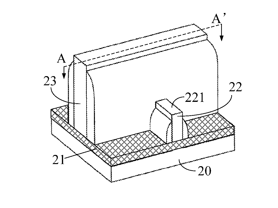
[0017]The existing FinFETs may have a relatively severe short channel effect and leakage current issue. Thus, the performance of the FinFETs may be adversely affected; and the FinFETs may be unable to match the performance requirements for developing ICs. Further, the existing FinFETs may accumulate a large amount of heat inside, i.e., self-heating effect, during the operation. The relatively bad heat dissipation may also affect the performance of the FinFET.

[0018]The leakage current issue of the FinFET may be caused by the relatively weak control ability of the gate to the carriers under the fin. The accumulation of the relatively large amount of heat may be caused by the structure of the existing FinFET. Silicon oxide may be used...


PUM

PropertyMeasurementUnit
temperatureaaaaaaaaaa
flow rateaaaaaaaaaa

Abstract

The present disclosure provides semiconductor devices, fin field-effect transistors and fabrication methods thereof. An exemplary fin field-effect transistor includes a semiconductor substrate; an insulation layer configured for inhibiting a short channel effect and increasing a heat dissipation efficiency of the fin field-effect transistor formed over the semiconductor substrate; at least one fin formed over the insulation layer; a gate structure crossing over at least one fin and covering top and side surfaces of the fin formed over the semiconductor substrate; and a source formed in the fin at one side of the gate structure and a drain formed in the fin at the other side of the gate structure.

Description

CROSS-REFERENCES TO RELATED APPLICATIONS[0001]This application claims the priority of Chinese patent application No. 201510293006.7, filed on Jun. 1, 2015, the entirety of which is incorporated herein by reference.FIELD OF THE INVENTION[0002]The present invention generally relates to the field of semiconductor technology and, more particularly, relates to semiconductor devices, fin field-effect transistors and fabrication processes thereof.BACKGROUND[0003]With the rapid development of semiconductor manufacturing technology, the technical node of the conventional integrated circuits (ICs) has been continuously shrunk. The critical dimension (CD) of the IC devices has become smaller and smaller. Correspondingly, the fabrication technique of the IC devices has been continuously improved so as to enhance the performances of the IC devices.[0004]For example, in an MOS transistor, a metal layer is usually formed between a high-dielectric constant (high-K) dielectric layer and a metal gate...

Claims


Application Information

Patent Timeline
Patent Type & Authority Applications(United States)
IPC IPC(8): H01L27/12H01L21/308H01L21/02H01L23/367H01L21/306H01L21/762H01L29/06H01L21/84H01L21/3065
CPCH01L27/1211H01L21/845H01L21/3081H01L21/02164H01L21/0223H01L23/367H01L21/30604H01L21/0234H01L21/02332H01L21/7624H01L29/0649H01L21/3065H01L29/1066H01L29/66409H01L29/785H01L2229/00H01L21/0214H01L21/02238H01L21/02252H01L21/3086H01L29/66795
Inventor XIE, XINYUNZHOU, MING
Owner SEMICON MFG INT (SHANGHAI) CORP
Why Eureka
Try Eureka