
Flash memory and method for receiving data therein

A technology of flash memory and random access memory, applied in the field of electronics, can solve the problems of a lot of cost, time-consuming copying, discontinuous data, etc., and achieve the effect of improving efficiency

Active Publication Date: 2015-09-30
SLICONGO MICROELECTRONICS INC
View PDF4 Cites 0 Cited by
  • Summary
  • Abstract
  • Description
  • Claims
  • Application Information

AI Technical Summary

Problems solved by technology

[0008] However, this method uses a physical block as a cache block for receiving HOST logical data. If the file system data and file data are written alternately, the above data is still discontinuous, and it still takes a lot of time to sort out and move the data into a composition. state of a data block
[0009] With the development of NAND FLASH technology, the development trend of NAND FLASH is from SLC (SingleLevel Cell, single-layer cell) to MLC (Multi-Level Cell multi-layer cell) to TLC (Trinary-Level Cell, three-layer cell), its single BLOCK contains more and more pages, the capacity of a single page is getting bigger and bigger, copying takes more and more time, and the efficiency is getting lower and lower

Method used


Image

  • Flash memory and method for receiving data therein
  • Flash memory and method for receiving data therein
  • Flash memory and method for receiving data therein

Examples


Embodiment Construction

[0028] In order to make the object, technical solution and advantages of the present invention clearer, the present invention will be further described in detail below in conjunction with the accompanying drawings and embodiments. It should be understood that the specific embodiments described here are only used to explain the present invention, not to limit the present invention.

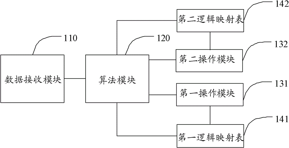
[0029] An embodiment of the present invention provides a flash memory, such as figure 1 As shown, the flash memory is provided with a first operating module 131 and a second operating module 132, and the RAM (random data memory) of the flash memory is provided with a first logical mapping table 141 and a second logical mapping table 142 , the flash memory includes:

[0030] A data receiving module 110, configured to receive logical data sent from the host;

[0031] The algorithm module 120 is used to judge whether the logical data is large data or small data, and if it is large data, write the la...


PUM


Abstract

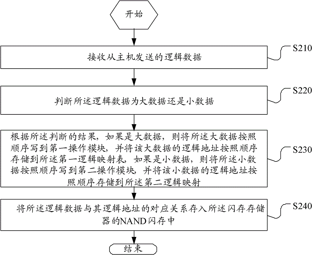
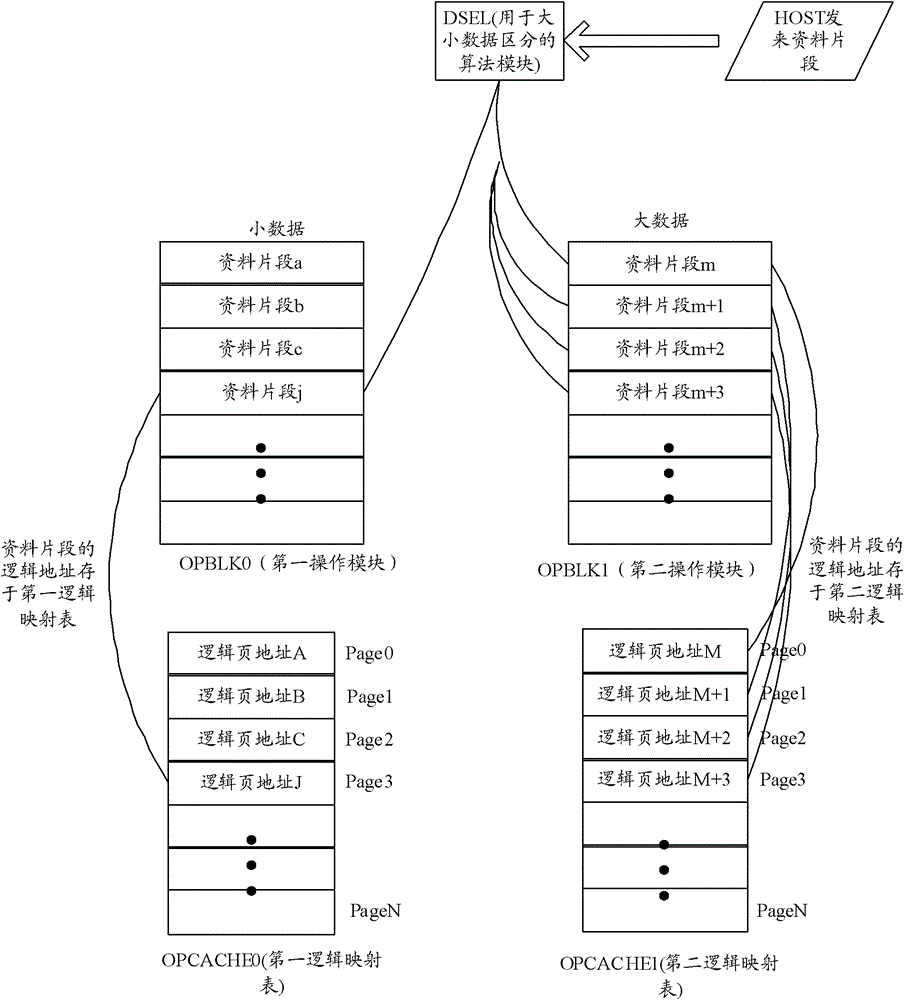
The invention relates to a flash memory and a data receiving method thereof. The flash memory is provided a first operation module and a second operation module; and the random-access memory (RAM) of the flash memory is provided with a first logic mapping table and a second logic mapping table. The method comprises: receiving logic data sent by master and slave computers; judging whether the logic data are big data or small data; and if the logic data are big data, writing the big data into the first operation module according to a sequence and storing the logic address of the big data into the first logic mapping table according to a sequence, or if the logic data are small data, writing the small data to a second operation module according to a sequence, storing the logic address of the small data into the second logic mapping table according to a sequence, and storing the corresponding relationship between the physical address of the logic data and the logic address of the logic data into the not and (NAND) flash of the flash memory. The flash memory and the data receiving method avoid preparing and transferring the logic data and improve the efficiency of the storage of discontinuous logic data.

Description

technical field [0001] The invention relates to the field of electronic technology, in particular to a flash memory and a method for receiving data thereof. Background technique [0002] The storage medium used for flash memory is mainly NANDFLASH (non-flash memory), and the composition relationship of NANDFLASH is: multiple pages (PAGE) form a block (BLOCK), and multiple blocks form a DEVICE (device), such as Samsung's MLC FLASH: The composition relationship of K9GAG08U0M is: each PAGE is 4K byte in size, 128 PAGEs constitute a BLOCK, the smallest unit for writing data is PAGE, and the smallest unit for erasing is BLOCK. After the data is written on the page, the entire block must be erased before the data can be rewritten. [0003] The mainstream method of managing the flash memory is block management: the flash memory divides the logical data sent by the HOST (host) into several logical data blocks, and the size of each logical data block is the same as that of the NAND ...

Claims


Application Information

Patent Timeline
Patent Type & Authority Patents(China)
IPC IPC(8): G06F12/08G06F12/02
Inventor 谭四方陈强吴大畏
Owner SLICONGO MICROELECTRONICS INC
Learn More