Semiconductor device

A semiconductor and circuit layer technology, applied in the field of semiconductor devices with a thermoelectric cooling mechanism, can solve the problems of insufficient heat dissipation efficiency of high-density packaging components, and achieve the effect of easy heat dissipation

Inactive Publication Date: 2012-07-04
IND TECH RES INST
View PDF4 Cites 10 Cited by
  • Summary
  • Abstract
  • Description
  • Claims
  • Application Information

AI Technical Summary

Problems solved by technology

[0004] The object of the present invention is to provide a semiconductor device that can solve the problem of insufficient heat dissipation efficiency of high-density packaging components

Method used


Image

  • Semiconductor device
  • Semiconductor device
  • Semiconductor device

Examples


Embodiment Construction

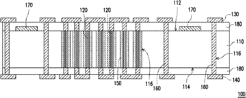
[0042] figure 1 is a cross-sectional view of a semiconductor device according to an embodiment of the present invention. Please refer to figure 1 The semiconductor device 100 of this embodiment includes a silicon substrate 110 , a plurality of silicon nanowire bundles 120 , a first circuit layer 130 and a second circuit layer 140 . The silicon substrate 110 has a first surface 112 and a second surface 114 opposite to each other and a plurality of through holes 116 . Each silicon nanowire bundle 120 is disposed in a through hole 116 . The first circuit layer 130 is disposed on the first surface 112 and electrically connected to the silicon nanowire bundle 120 . The second circuit layer 140 is disposed on the second surface 114 and electrically connected to the silicon nanowire bundle 120 .

[0043] In this embodiment, the silicon nanowire bundle 120 is, for example, directly fabricated from the silicon substrate 110 . Each silicon nanowire bundle 120 is, for example, a P-t...


PUM


Abstract

A semiconductor device including a silicon substrate, a plurality of silicon nanowire clusters, a first circuit layer and a second circuit layer. The silicon substrate has a first surface, a second surface opposite to the first surface and a plurality of through holes. The silicon nanowire clusters are disposed in the through holes of the silicon substrate, respectively. The first circuit layer is disposed on the first surface and connected to the silicon nanowire clusters. The second circuit layer is disposed on the second surface and connected to the silicon nanowire clusters.

Description

technical field [0001] The present invention relates to a semiconductor device, and more particularly to a semiconductor device with a thermoelectric cooling mechanism. Background technique [0002] The future trend of packaging manufacturing technology will be towards high-precision manufacturing technology such as high power, high density, low cost, light, thin, short, and small, and the technology of 3D stacked IC (3D stacked IC) is for this purpose , one of the most serious challenges is the problem of heat. The formation of local high-temperature regions and hot spots in the 3D stacked chip will cause temperature and stress concentration and lead to thermal stress problems, which will affect the reliability of the product and become the bottleneck of the 3D stacked chip technology. According to the research, the hot spot problem will greatly increase the heat dissipation demand of the chip, so that the thermal resistance value of the heat dissipation element needs to b...

Claims


Application Information

Patent Timeline
Patent Type & Authority Applications(China)
IPC IPC(8): H01L23/36H01L23/367H01L23/373
CPCH01L2924/0002H01L2225/06513H01L2225/06589H01L2225/06541H01L23/53276H01L21/76898H01L23/38H01L23/481H01L25/0657H01L2224/16H01L2221/1094
Inventor 刘君恺刘汉诚戴明吉谭瑞敏
Owner IND TECH RES INST
Why Eureka
Try Eureka