
Photovoltaic bypass protection device

A bypass protection, photovoltaic technology, applied in the field of photovoltaics, can solve the problems of long cable length, burnout components, increase the probability of abnormality and resistance loss, etc., to reduce the probability of abnormality and resistance loss, reduce the probability of abnormality, Reduces the effect of electrical connection contacts

Active Publication Date: 2014-01-22
苏州固锝新能源科技有限公司
View PDF4 Cites 0 Cited by
  • Summary
  • Abstract
  • Description
  • Claims
  • Application Information

AI Technical Summary

Problems solved by technology

If the protection device is damaged or the connection is not reliable, the protection device will not work properly, so when the solar module is partially blocked, the entire solar module system will not work normally, and the hot spot effect will cause a large amount of heat to be generated by the battery sheet. In severe cases, it will burn bad components, so in photovoltaic devices, the position of photovoltaic bypass protection device is very important
[0003] In the prior art, the disadvantage of similar device structures is that when loading bus bars, the whole device must first be glued to the surface of the photovoltaic module, so it is difficult to operate during the installation process. Correspondingly, once the device needs to be dismantled , it is necessary to remove the fixing strip from the surface of the photovoltaic module, which may damage the connection surface, and the process is cumbersome; again, the existing device, such as the Chinese patent application number 201110297543. The cavity is located on both sides of the pins used to connect with the bus bar in the working circuit module (201). More electrical connection contacts, greatly increasing the probability of abnormality and resistance loss

Method used


Image

  • Photovoltaic bypass protection device
  • Photovoltaic bypass protection device
  • Photovoltaic bypass protection device

Examples


Embodiment Construction

[0024] The preferred embodiments of the present invention will be described in detail below in conjunction with the accompanying drawings, so that the advantages and features of the present invention can be more easily understood by those skilled in the art, so as to define the protection scope of the present invention more clearly.

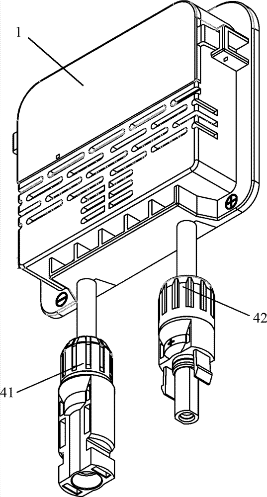
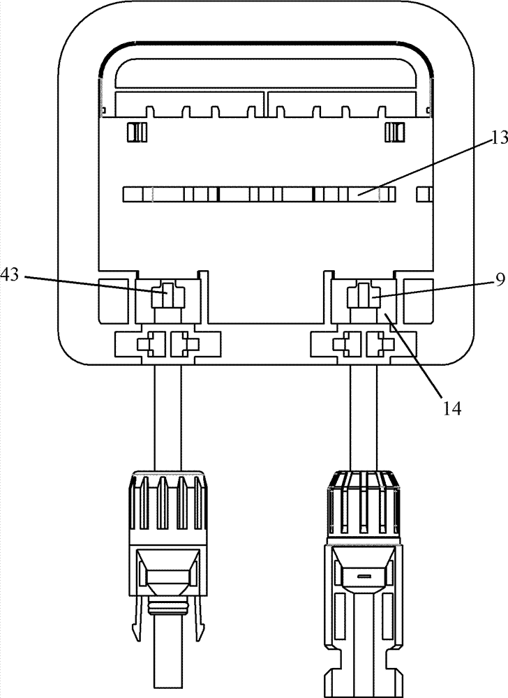
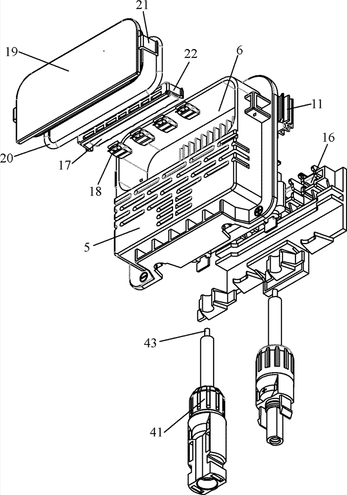
[0025] See attached Figure 1-6 , the photovoltaic bypass protection device in this embodiment includes a main body 1, a working circuit module 2, a heat dissipation module 3, and connection modules 41 and 42 with terminals 43, and the main body 1 has an accommodating cavity 5 and a sealing cavity 6; The sealed cavity 6 is gas-liquid sealed from the outside world. The working circuit module 2 includes a substrate 7 with a built-in working circuit. The working circuit extends from one side of the substrate 7 with several first pins 8 extending from the other side of the substrate 7. There are two second pins 9, the first pin 8 has a bent end surfa...


PUM


Abstract

The invention discloses a photovoltaic bypass protection device. The photovoltaic bypass protection device comprises a main body, an operating circuit module, a heat radiating module and a connecting module with a wiring terminal, wherein the main body is provided with an accommodating cavity and a sealed cavity; the operating circuit module comprises a first pin and a second pin; the front segment of a substrate is embedded into a ring-shaped radiator with a plurality of radiating fins arranged on the outer surface; the ring-shaped radiator and the front segment of the substrate are embedded into the accommodating cavity; the rear segment of the substrate is positioned in a first glue injection cavity between the accommodating cavity and the seal cavity; a second glue injection cavity for placing both the wiring terminal and the second pin is formed at the front end of the accommodating cavity; the first glue injection cavity and the second glue injection cavity are filled with sealant; and the bent end surface of the first pin is positioned in a positioning groove. The photovoltaic bypass protection device provided by the invention has the advantages of reduced size, lower cable consumption, less electric connection contacts, and low abnormity probability and resistance loss, and the sealed cavity allowing water vapor from the wiring terminal to enter is effectively arranged.

Description

technical field [0001] The invention relates to a photovoltaic bypass protection device, which belongs to the photovoltaic field. Background technique [0002] Photovoltaic cells are devices that directly convert solar radiation energy into electrical energy. Photovoltaic modules are products that are connected and packaged by multiple photovoltaic cells. They are the basic units of battery arrays in photovoltaic power generation systems. The photovoltaic module bypass integrated protection device is a key connection device for the solar module system. The function of the device is to prevent the hot spot effect when the solar module is partially blocked. If the protection device is damaged or the connection is not reliable, the protection device will not work properly, so when the solar module is partially blocked, the entire solar module system will not work normally, and the hot spot effect will cause the battery to generate a lot of heat, which will seriously burn There...

Claims


Application Information

Patent Timeline
Patent Type & Authority Patents(China)
IPC IPC(8): H02S40/36H02S40/42H02S40/34
CPCY02E10/50Y02A30/14
Inventor 陈新初吴念博滕有西李志军张雄杰何耀喜顾德圣相鸿彬余觉
Owner 苏州固锝新能源科技有限公司
Learn More