Method for manufacturing light emitting diode (LED) grains

A technology of light-emitting diodes and manufacturing methods, which is applied to electrical components, circuits, semiconductor devices, etc., and can solve problems such as reducing the light-emitting efficiency of light-emitting diode crystal grains

Inactive Publication Date: 2012-07-04
ZHANJING TECH SHENZHEN +1
View PDF5 Cites 5 Cited by
  • Summary
  • Abstract
  • Description
  • Claims
  • Application Information

AI Technical Summary

Problems solved by technology

However, the above-mentioned structure has the following problems: the light emitted by the semiconductor light-emitting structure toward the substrate side will be absorbed by the substrate and converted into heat energy after entering the substrate, thereby reducing the light extraction efficiency of the light-emitting diode crystal grains

Method used


Image

  • Method for manufacturing light emitting diode (LED) grains
  • Method for manufacturing light emitting diode (LED) grains
  • Method for manufacturing light emitting diode (LED) grains

Examples


Embodiment Construction

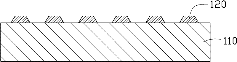
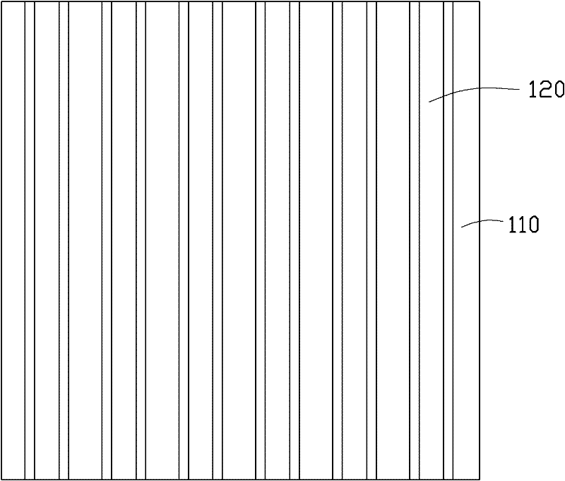
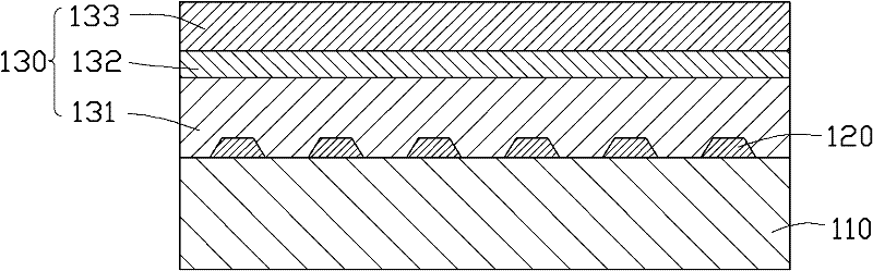
[0039] Such as figure 1 As shown, a sapphire substrate 110 is provided first. Then a silicon dioxide pattern layer 120 is fabricated on the sapphire substrate 110 . See figure 2 , the silicon dioxide pattern layer 120 is composed of a plurality of strip-shaped silicon dioxide patterns arranged in parallel. Such as image 3 As shown, the cross-sectional shape of the elongated silicon dioxide pattern perpendicular to its extending direction is trapezoidal. According to requirements, the cross-sectional shape of the elongated silicon dioxide pattern along the direction perpendicular to its extension can also be a semicircle.

[0040] Such as image 3 As shown, the semiconductor light emitting structure 130 is grown on the surface of the sapphire substrate 110 with the silicon dioxide pattern layer 120 by Metal Organic Chemical Vapor Deposition (MOCVD) or Molecular Beam Epitaxy (MBE). The semiconductor light emitting structure 130 includes an n-type GaN layer 131 , a multi-...


PUM


Abstract

The invention relates to a method for manufacturing light emitting diode (LED) grains. A silicon dioxide pattern layer is formed at the bottoms of the LED grains and is removed by buffered oxide etch to form penetrating holes after the growth of a semiconductor light emitting structure is finished; and through the penetrating holes, the probability that light rays which are emitted by the semiconductor light emitting structure and face a sapphire substrate are emitted upwards through total reflection can be improved, so that the light emitting efficiency of the LED grains is improved.

Description

technical field [0001] The invention relates to a method for manufacturing a light-emitting diode crystal grain, in particular to a method for manufacturing a light-emitting diode crystal grain with high light extraction efficiency. Background technique [0002] A light emitting diode (Light Emitting Diode, LED) is a semiconductor element that can convert electric current into light in a specific wavelength range. Light-emitting diodes can be widely used as light sources in the field of lighting because of their advantages such as high brightness, low operating voltage, low power consumption, easy matching with integrated circuits, simple driving, and long life. [0003] Existing light-emitting diode grains generally include a substrate and a semiconductor light-emitting structure grown on the surface of the substrate. However, the above structure has the following problem: the light emitted by the semiconductor light-emitting structure towards the substrate will be absorbe...

Claims


Application Information

Patent Timeline
Patent Type & Authority Applications(China)
IPC IPC(8): H01L33/00H01L33/10H01L33/20
CPCH01L33/0095H01L33/20H01L33/007
Inventor HUANG SHISHENGTU BOMIN
Owner ZHANJING TECH SHENZHEN
Why Eureka
Try Eureka