Electric tunable grating coupler

A grating coupler and mode converter technology, applied in the coupling of optical waveguide, light guide, optics, etc., can solve the problems of efficiency drop, substantial increase, center wavelength shift, etc.

Active Publication Date: 2012-07-11
INST OF SEMICONDUCTORS - CHINESE ACAD OF SCI
View PDF5 Cites 32 Cited by
  • Summary
  • Abstract
  • Description
  • Claims
  • Application Information

AI Technical Summary

Problems solved by technology

Unfortunately, the efficiency of ordinary uniform gratings often has an upper limit, and it is difficult to greatly improve it only by changing the grating parameters. Moreover, due to the influence o...

Method used


Image

  • Electric tunable grating coupler
  • Electric tunable grating coupler
  • Electric tunable grating coupler

Examples


Embodiment Construction

[0027] specific implementation plan

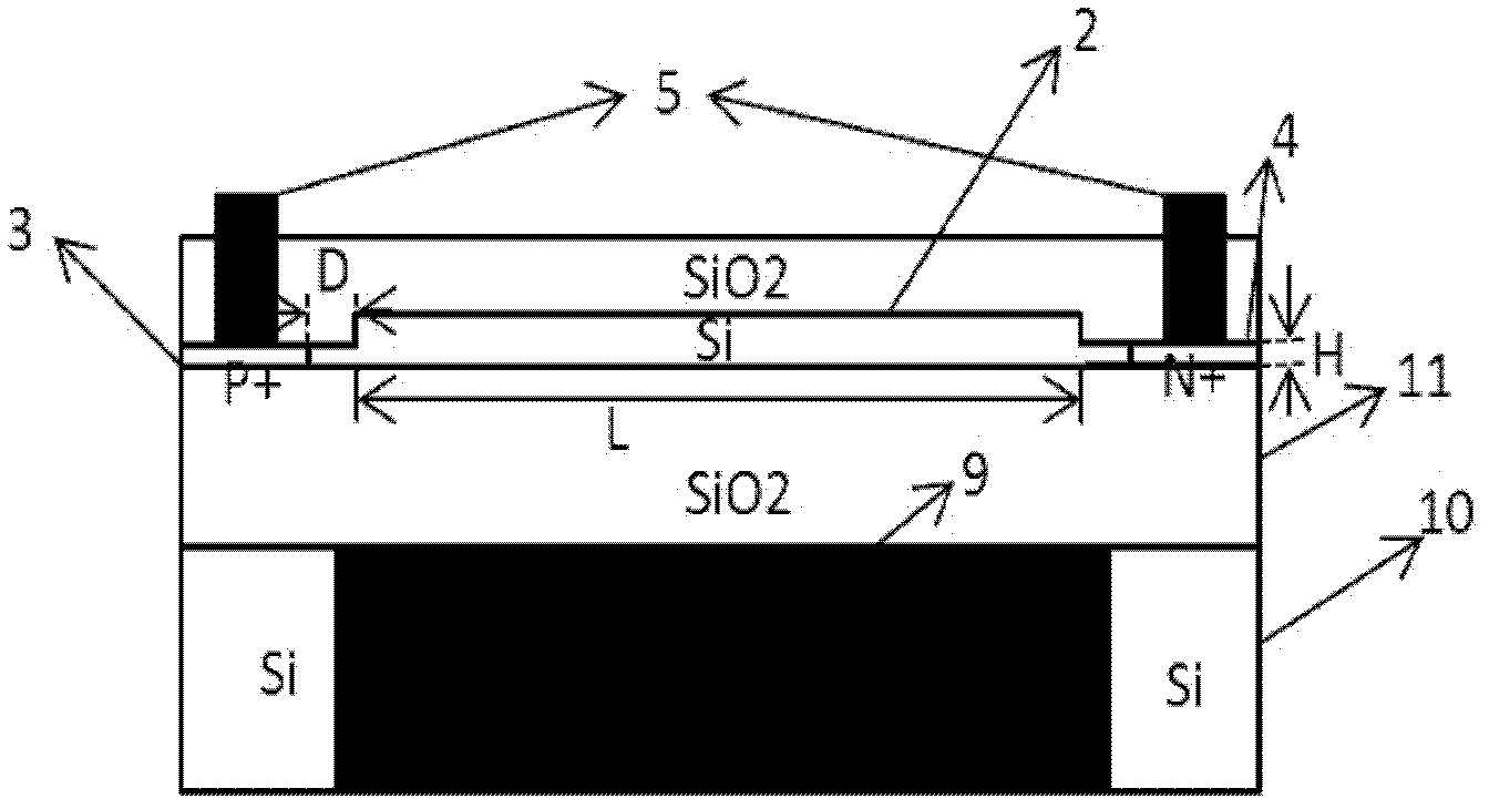
[0028]Since the present invention is a silicon-based tunable grating coupler designed based on the SOI substrate material, for different thicknesses of the buried oxide layer and the thickness of the top layer of silicon, the corresponding optimal design is also different in order to achieve the functional requirements. Therefore, for the convenience of description, this The substrate material of the invention defaults to specific implementation parameters, that is, the thickness of the buried oxide layer is 2 μm, and the thickness of the top silicon layer is 220 nm.

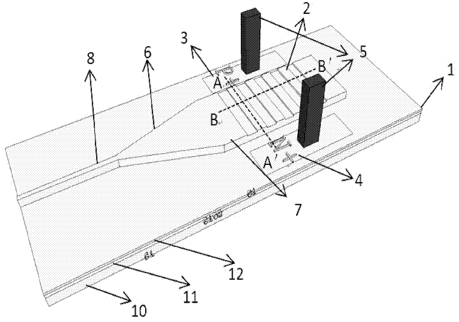
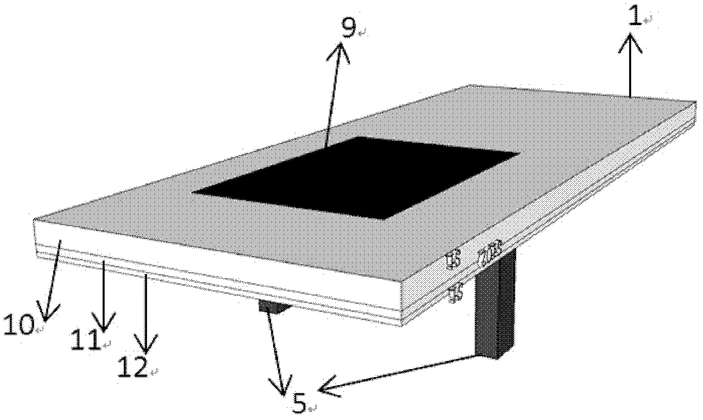
[0029] Figure 1a , Figure 1b It is a schematic diagram of the three-dimensional effect of the present invention, and is a schematic diagram of the front and reverse sides of the present invention respectively. Referring to this figure, it can be seen that the present invention provides an electrically tunable grating coupler, including:

[0030] An SOI substrate 1, inclu...


PUM


Abstract

The invention discloses an electric tunable grating coupler. The electric tunable grating coupler comprises an SOI (Silicon On Insulator) substrate, an oblique incidence grating coupler, a P+ mixing area, an N+ mixing area, a pair of electrodes, a mode converter, a single mode ridge waveguide and a substrate gold reflecting mirror, wherein the SOI substrate comprises a silicon substrate, an oxideburying layer and a top silicon layer positioned at the upper position of the SOI substrate; the oblique incidence grating coupler is positioned on the top silicon layer positioned on the SOI substrate; the P+ mixing area is positioned in a panel area at one side of the oblique incidence grating coupler; the N+ mixing area is positioned in the panel area at the other side of the oblique incidencegrating coupler; the electrodes are positioned at the upper positions of the P+ mixing area and the N+ mixing area, are respectively connected with the P+ mixing area and the N+ mixing area through metal contact through holes and are used for loading electric signals; one end of the mode converter is provided with a wide waveguide, the mode converter is positioned at one end of the oblique incidence grating coupler, and the end of the mode converter, which is provided with the wide waveguide, is coupled with one end of the oblique incidence grating coupler; the single mode ridge waveguide andthe oblique incidence grating coupler are respectively positioned at two ends of the mode converter; and the substrate gold reflecting mirror is embedded in the silicon substrate positioned at the bottom part of the SOI substrate and is positioned below the oblique incidence grating coupler and the oxide burying layer.

Description

technical field [0001] The invention relates to silicon-based optoelectronic technology, in particular to an SOI-based electrically tunable grating coupler. Background technique [0002] Microelectronics technology and optical fiber communication technology are the two cornerstones of human information society. In the past half century, with the development of integrated circuits, silicon-based materials and device technology have become surprisingly mature, and with the continuous shrinking of process feature sizes, the integration of integrated circuits has been developing rapidly in accordance with Moore's law. The higher integration of chips brings not only an increase in the number of transistors, but also an increase in chip functions and processing speed. For example, the latest 8-core microprocessor Nehalem-EX of Intel's 45nm process has 2.3 billion transistors. However, as feature sizes shrink and integration levels continue to increase, the limitations of microel...

Claims


Application Information

Patent Timeline
IPC IPC(8): G02B6/34G02B6/124
Inventor 陈弘达张赞允黄北举张赞
Owner INST OF SEMICONDUCTORS - CHINESE ACAD OF SCI
Why Eureka
Try Eureka