Method for detecting offset of focus of lithography machine

A technology of lithography machine and focal length, which is applied in the direction of testing optical performance, microlithography exposure equipment, and photolithography exposure equipment, etc. It can solve the problems of high measurement position requirements, production loss, and final result interference, so as to avoid judgment effect of error

Active Publication Date: 2014-02-05
SHANGHAI HUALI MICROELECTRONICS CORP
View PDF5 Cites 0 Cited by
  • Summary
  • Abstract
  • Description
  • Claims
  • Application Information

AI Technical Summary

Problems solved by technology

[0003] In the lithography process, if the focal length of the lithography machine cannot be detected in time, it will bring huge losses to the production; the existing technology mainly uses the method of measuring key dimensions or measuring the overlay accuracy for monitoring, but A special exposure of a wafer is required to monitor the condition of the machine, and at the same time, the measurement of key dimensions has relatively high requirements on the measurement position. When the measurement position changes, it will bring great interference to the final result.

Method used


Image

  • Method for detecting offset of focus of lithography machine
  • Method for detecting offset of focus of lithography machine
  • Method for detecting offset of focus of lithography machine

Examples


Embodiment Construction

[0018] The specific embodiment of the present invention will be further described below in conjunction with accompanying drawing:

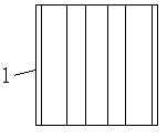
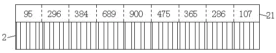
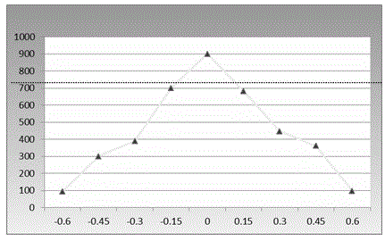
[0019] figure 1 It is a schematic structural diagram of a reference figure in the method for detecting focal length offset of a lithography machine according to the present invention; figure 2 It is a schematic structural diagram of a test pattern in the method for detecting focal length offset of a lithography machine according to the present invention; image 3 It is a graph of the relationship between the similarity score and the focal length of the lithography machine in the method for detecting the focal length offset of the lithography machine in the present invention; Figure 4 It is a schematic diagram of the pattern on the wafer after exposure and its similarity score in the actual process of the method for detecting the focal length offset of the lithography machine of the present invention.

[0020] Such as Figure 1-4 As shown, a m...


PUM


Abstract

The invention relates to the field of semiconductor manufacturing, in particular to a method for detecting offset of focus of a lithography machine. According to the method for detecting the offset of the focus of the lithography machine, the offset of the focus of the lithography machine is monitored by depending on monitoring the similarity level of an actual measurement graph and a reference graph, the change condition of the focus of the lithography machine can be immediately and effectively judged through measuring massively-produced wafers, and measurement interference can be avoided, thus judgment errors caused by the measurement errors are avoided.

Description

technical field [0001] The invention relates to the field of semiconductor integrated circuits and the manufacture thereof, in particular to a method for detecting focal length offset of a photolithography machine. Background technique [0002] As the integration level of integrated circuits continues to increase, semiconductor technology continues to develop rapidly. With the continuous improvement of semiconductor performance requirements, the size of integrated circuit chips is getting smaller and smaller, and the photolithography process has gradually become the core process in chip manufacturing. Usually, in a complete chip manufacturing process, multiple photolithography processes are required. For example, in a complete 45nm process chip manufacturing process, about 40 to 60 photolithography processes are required depending on the performance requirements; As the size shrinks, the pattern of lithography will also shrink accordingly, and the thickness of photoresist a...

Claims


Application Information

Patent Timeline
Patent Type & Authority Patents(China)
IPC IPC(8): G03F7/20G01M11/02
Inventor 夏婷婷毛智彪马兰涛
Owner SHANGHAI HUALI MICROELECTRONICS CORP
Why Eureka
Try Eureka