Manufacturing method for flexible and hard combined thin PCB

A soft-hard combination and processing method technology, applied in the direction of assembling printed circuits with electrical components, can solve problems such as affecting the quality of the board, damage to the window, and inability to manufacture, and achieve the effect of improving the pass rate and simplifying the processing process.

Active Publication Date: 2012-07-11
SHANGHAI MEADVILLE ELECTRONICS
View PDF3 Cites 21 Cited by
  • Summary
  • Abstract
  • Description
  • Claims
  • Application Information

AI Technical Summary

Problems solved by technology

Each step of the process may damage the corresponding copper foil at the window 21 and window 41
Especially during etching, the copper foil at the corresponding positions of window 21 and window 41 will have a serious problem of copper breakage, causing the circuit pattern of the soft board to be etche

Method used


Image

  • Manufacturing method for flexible and hard combined thin PCB
  • Manufacturing method for flexible and hard combined thin PCB
  • Manufacturing method for flexible and hard combined thin PCB

Examples


Embodiment Construction

[0036] The present invention is described in detail below in conjunction with embodiment:

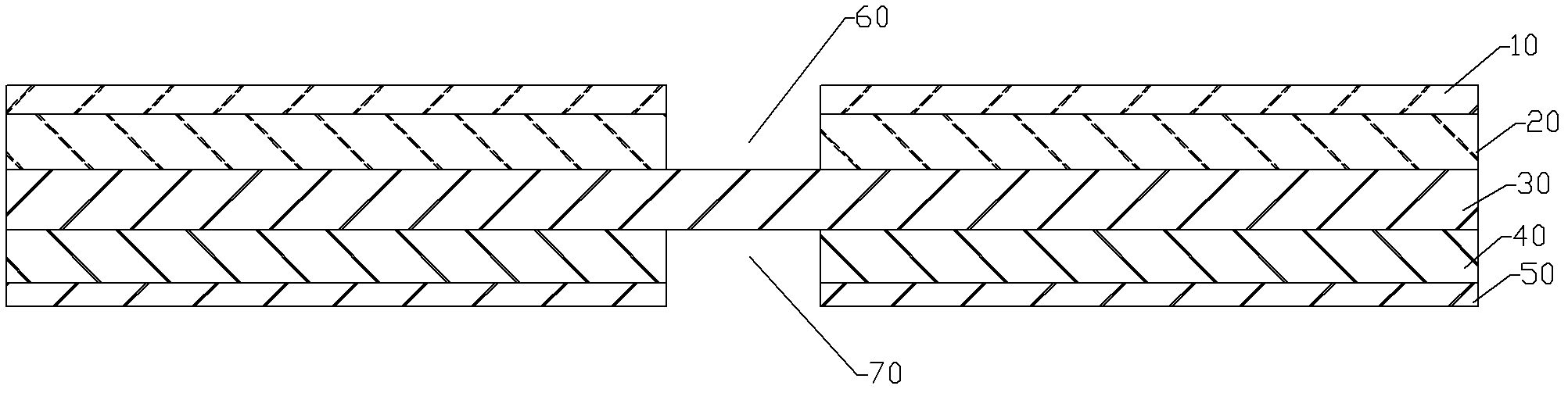
[0037] Taking the processing of a 0.2mm thick flexible and rigid PCB sheet as an example, the processing method of a flexible and rigid PCB sheet, steps a-d are as follows image 3 , Figure 4 shown.

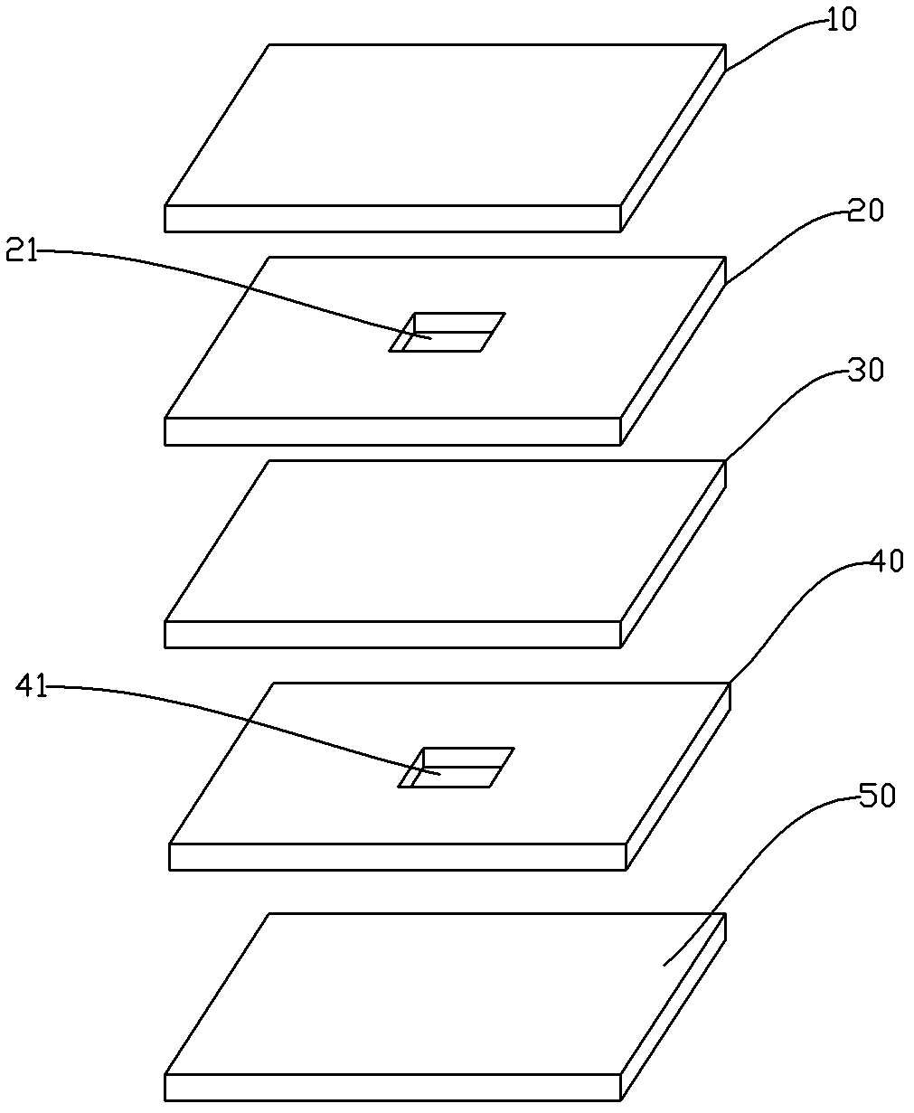
[0038] a. Provide a soft board 3 with circuit patterns on both sides.

[0039] b. Silk-print liquid PI on the position to be protected on the upper surface of the flexible board 3 , and silk-screen print liquid PI on the position to be protected on the lower surface. The liquid PI is pre-cured by drying. A first protective film 81 is formed on the upper surface of the flexible board 3 ; a second protective film 82 is formed on the lower surface.

[0040] c. Providing the first prepreg 2 and the second prepreg 4 . Using UV laser or CO 2 The laser milling method mills through the first prepreg 2 to form the window 22 on the first prepreg 2 . Using UV laser or CO 2 The laser milling ...


PUM


Abstract

The invention discloses a manufacturing method for a flexible and hard combined thin PCB, and is characterized by comprising the steps as follows: a) a flexible board with a circuit graphs on the surface thereof is provided; b) a protective film is arranged on the surface of the flexible board provided with the circuit graphs; c) prepregs with windows are provided, the prepregs are stacked on the surface of the flexible plate, and the protective film corresponds to the position of the windows of the pregregs; d) hard boards are provided and stacked on the surfaces of the prepregs, and the prepregs are located among the flexible board and the hard boards; e) the laminating is carried out; and f) the parts of the hard boards corresponding to the position of the protective film are removed. The invention has the benefits that a first hard board and a second hard board located on the most outer layers of the thin PCB can only adopt copper foil, and the problem that an etching solution provided by the copper foil damages the circuit graphs on the flexible board is solved, so that the manufacturing of thinner PCBs is achieved; and after manufacturing the flexible plate, a protective layer is not required before manufacturing the flexible and hard combined thin PCB, and the procedure of the manufacturing is simplified.

Description

technical field [0001] The invention relates to a method for processing a soft-hard PCB thin plate. Background technique [0002] The soft and hard PCB board is a printed circuit board composed of a flexible circuit board, that is, a soft board, and a rigid circuit board, that is, a hard board. Its structure can be divided into three layers, four layers or more than five layers. Such as figure 1 Shown is a cross-sectional view of a rigid-flex PCB with a four-layer structure. The first hard board 10 , the first prepreg 20 , the soft board 30 with circuit patterns on both sides, the second prepreg 40 and the second hard board 50 are arranged and laminated in sequence. The circuit pattern on the flexible board 10 corresponding to the first window 60 and the second window 70 can be exposed. The first hard board 10 and the second hard board 50 are polymer material boards with copper foil attached to one side. It has a total of four layers of copper foil, so its structure is ...

Claims


Application Information

Patent Timeline
IPC IPC(8): H05K3/36
Inventor 屈刚瞿长江
Owner SHANGHAI MEADVILLE ELECTRONICS
Why Eureka
Try Eureka