Phase change memory cell and producing method thereof

A technology of phase change storage and manufacturing method, which is applied in the field of phase change storage unit introducing high-resistance materials and its production, which can solve problems such as failure and performance degradation of phase change storage unit, so as to avoid excessive corrosion, improve storage performance and finished products rate effect

Active Publication Date: 2012-07-18
SHANGHAI INST OF MICROSYSTEM & INFORMATION TECH CHINESE ACAD OF SCI
View PDF4 Cites 5 Cited by
  • Summary
  • Abstract
  • Description
  • Claims
  • Application Information

AI Technical Summary

Problems solved by technology

[0005] The purpose of the present invention is to provide a phase-change memory unit and a manufacturing method thereof, which are used to solve the problem that the performance of the phase-change memory unit is reduced or even caused by the excessive corrosion of the phase-change material in the phase-change memory unit in the prior art during chemical mechanical polishing. failure problem

Method used


Image

  • Phase change memory cell and producing method thereof
  • Phase change memory cell and producing method thereof
  • Phase change memory cell and producing method thereof

Examples


no. 1 example

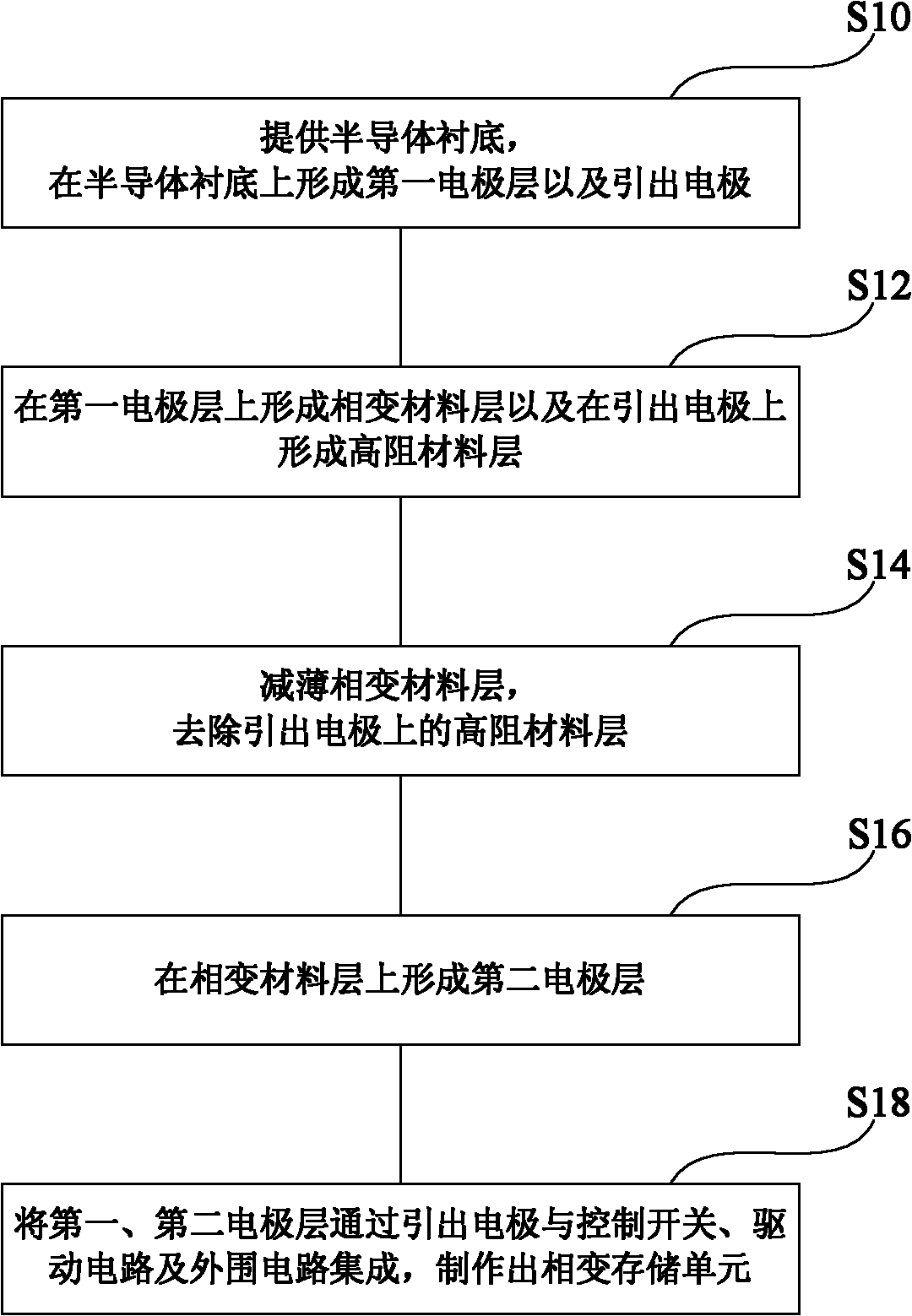
[0027] see figure 2 , which shows a schematic flow chart of the first embodiment of the manufacturing method of the phase-change memory cell provided by the present invention. like figure 2 As shown, the preparation method includes the following steps:

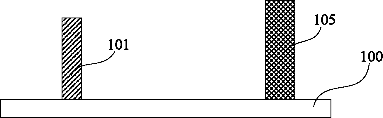
[0028] S10, providing a semiconductor substrate, forming a first electrode layer and an extraction electrode on the semiconductor substrate;

[0029] S12, forming a phase-change material layer on the first electrode layer and forming a high-resistance material layer on the extraction electrode;

[0030] S14, thinning the phase change material layer, and removing the high resistance material layer on the extraction electrode;

[0031] S16, forming a second electrode layer on the phase change material layer;

[0032] S18, integrating the first and second electrode layers with the control switch, drive circuit and peripheral circuits through the lead-out electrodes to manufacture a phase-change memory unit.

[0033] The co...

no. 2 example

[0053] see Figure 9 , which shows a schematic flow chart of the first embodiment of the manufacturing method of the phase-change memory cell provided by the present invention. like Figure 9 As shown, the preparation method includes the following steps:

[0054] S20, providing a semiconductor substrate, forming a first electrode layer and an extraction electrode on the semiconductor substrate;

[0055] S22, forming a high resistance material layer on the first electrode layer;

[0056] S24, forming a phase change material layer on the high resistance material layer and performing thinning treatment;

[0057] S26, forming a second electrode layer on the phase change material layer;

[0058] S28 , integrating the first and second electrode layers with the control switch, drive circuit and peripheral circuits through the lead-out electrodes to manufacture a phase-change memory unit.

[0059] The content of the present invention will be described in detail below in conjuncti...


PUM

PropertyMeasurementUnit
thicknessaaaaaaaaaa
thicknessaaaaaaaaaa
thicknessaaaaaaaaaa

Abstract

The invention provides a phase change memory cell and a producing method thereof, the phase change memory cell comprises a semiconductor substrate, a first electrode layer, a phase-change material layer, a second electrode layer, an extraction electrode and a high-resistance material layer, wherein the high-resistance material layer is used for preventing the phase-change material layer from being excessively corroded in the process of chemical mechanical polishing, the resistance of the high-resistance material layer is at least ten times of or above that of the phase-change material layer, the phase-change material layer can be prevented from being excessively corroded in the process of chemical mechanical polishing and the memory performance and yield of the phase change memory cell are increased.

Description

technical field [0001] The invention relates to a phase-change storage technology, in particular to a phase-change storage unit introduced with high-resistance materials and a manufacturing method thereof. Background technique [0002] Phase-change memory (PC-RAM) is a non-volatile semiconductor memory that has emerged in recent years. It is based on Ovshinsky's research in the late 1960s (Phys. Rev. Lett., 21, 1450-1453, 1968) and early 1970s ( Appl. Phys. Lett., 18, 254-257, 1971) put forward the idea that the phase-change film can be applied to the phase-change storage medium, and it is a storage device with low price and stable performance. Phase-change memory can be made on a silicon wafer substrate, and its key materials are recordable phase-change films, heating electrode materials, heat insulating materials, and lead-out electrode materials. The basic principle of phase change memory is to use electric pulse signal to act on the device unit, so that the phase change...

Claims


Application Information

Patent Timeline
Patent Type & Authority Applications(China)
IPC IPC(8): H01L45/00
CPCH01L45/16H01L45/149H01L45/06H01L45/148H01L45/1616H01L27/2463H01L45/1253H01L45/141H01L45/1666H01L45/145H01L45/144H01L45/1233G11C13/0004H10N70/231H10N70/826H10N70/8828H10N70/026H10N70/066H10N70/011H10N70/841
Inventor 刘波宋志棠张挺李莹钟旻封松林
Owner SHANGHAI INST OF MICROSYSTEM & INFORMATION TECH CHINESE ACAD OF SCI
Why Eureka
Try Eureka