

Solar cell substrate, manufacturing method of solar cell and crucible used for same
A technology of solar cells and crucibles, applied in chemical instruments and methods, circuits, electrical components, etc., can solve problems such as difficulty in matching corrosive agents
- Summary
- Abstract
- Description
- Claims
- Application Information
AI Technical Summary
Problems solved by technology
Method used
Image

Examples
Embodiment Construction
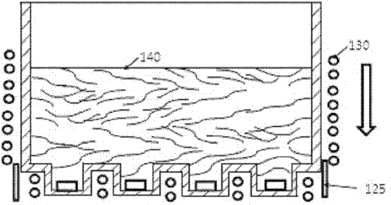
[0017] Embodiments of the present invention enable the production of solar cells at reduced cost while reducing health and environmental hazards in conventional solar cell manufacturing processes. Contrary to conventional teaching, the present invention discloses a method of using metallurgical grade silicon (MGSi) of 3N-5N purity to fabricate substrates and solar cells. Various embodiments of the present disclosure combine the benefits of crystalline silicon solar cells and thin film silicon solar cells based on thin film technology cells with conversion efficiencies greater than 16%. In order to improve the conversion efficiency, the short-circuit current, JC, is increased by texturizing the surface of the silicon wafer before fabricating the solar cell. By casting metallurgical-grade silicon on multiple crystals, the percentage of crystals can be increased to facilitate the texturing process.
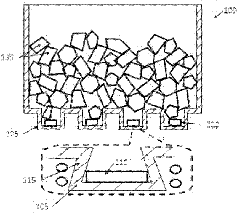
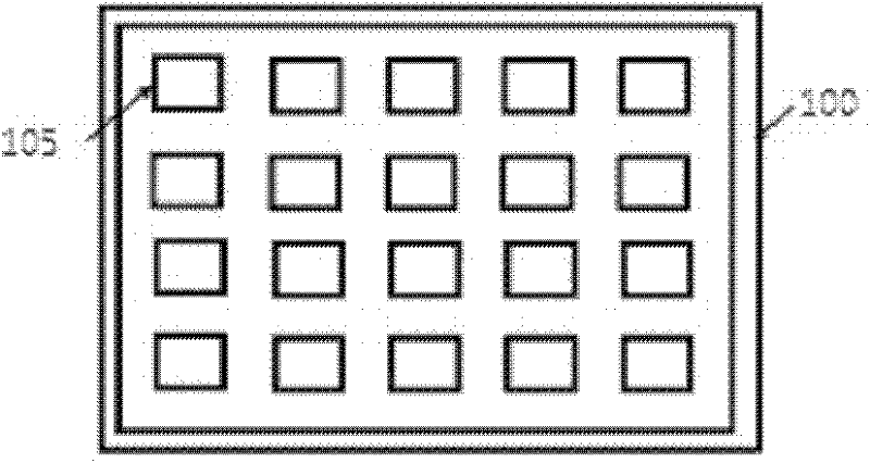
[0018] figure 1 is a casting crucible 100 shown according to an exemplary em...
PUM
 Abstract
Description
Claims
Application Information