Reflective GaA1As photoelectric cathode with sensitive peak response at 532nm and preparation method of reflective GaA1As photoelectric cathode

A peak response, photocathode technology, applied in cold cathode manufacturing, electrode system manufacturing, discharge tube/lamp manufacturing, etc., can solve the problems of narrow band response noise, cannot be used all-weather, wide cathode response band, etc., to reduce the interface The effect of recombination rate, reduction of growth interface stress, and improvement of interface properties

Inactive Publication Date: 2012-07-25
NANJING UNIV OF SCI & TECH
View PDF4 Cites 20 Cited by
  • Summary
  • Abstract
  • Description
  • Claims
  • Application Information

AI Technical Summary

Problems solved by technology

However, the blue extended cathode developed by our country's current laboratory has a spectral response of 110 mA/W at 532 nm, a quantum efficiency of 25%, and a full-spectrum integration sensitivity of less than 2000 μA/lm. This device has not yet been used in ocean detection, ocean communication,

Method used


Image

  • Reflective GaA1As photoelectric cathode with sensitive peak response at 532nm and preparation method of reflective GaA1As photoelectric cathode
  • Reflective GaA1As photoelectric cathode with sensitive peak response at 532nm and preparation method of reflective GaA1As photoelectric cathode
  • Reflective GaA1As photoelectric cathode with sensitive peak response at 532nm and preparation method of reflective GaA1As photoelectric cathode

Examples


Embodiment 1

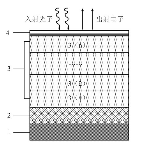
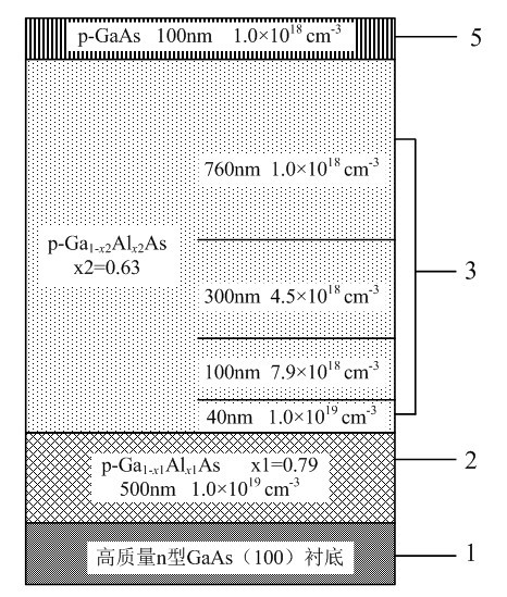
[0041] Step 1: In high quality (dislocation density ≤ 100 cm -2 ) On n-type GaAs(100) substrate 1, p-type doped Ga was grown by MOCVD epitaxy 1-x1 Al x1 As buffer layer 2, Ga 1-x1 Al x1 Al composition value of As buffer layer 2 x 1 is taken as 0.79, the total thickness is taken as 500 nm, the uniform doping method is adopted, the doping atoms are Zn, and the doping concentration is 1.0×10 19 cm -3 .

[0042] Step 2: In Ga 1-x1 Al x1 Epitaxial growth of Ga on As buffer layer 2 1-x2 Al x2 Emitter layer 3 with As doping concentration gradient, Ga 1-x2 Al x2 Al composition value of As emission layer 3 x 2 is taken as 0.63; by 4 p-type Ga 1-x Al x The unit layer composed of As epitaxial material, the thickness value of each unit layer changes according to the index, respectively designed as 40nm, 100 nm, 300 nm, 760 nm, Ga 1-x2 Al x2 The total thickness of the As doping concentration gradient emission layer is 1200 nm; the four units are all doped with Zn, and the ...

Embodiment 2

[0052] The first step: On the n-type GaAs(100) substrate, grow p-type doped Ga by MOCVD epitaxy 1-x1 Al x1 As buffer layer, Ga 1-x1 Al x1 Al composition value of As buffer layer x 1 is taken as 0.75, the total thickness is taken as 100 nm, the uniform doping method is adopted, the doping atoms are Zn, and the doping concentration is 1.0×10 19 cm -3 .

[0053] Step 2: In Ga 1-x1 Al x1 Epitaxial Growth of Ga on As Buffer Layer 1-x2 Al x2 Emitter layer with graded As doping concentration, Ga 1-x2 Al x2 Al composition value of As emission layer x 2 is taken as 0.68; by 4 p-type Ga 1-x Al x The unit layer composed of As epitaxial material, the thickness of each unit layer is designed to be 40nm, 100nm, 300nm, 760nm, Ga 1-x2 Al x2 The total thickness of the As doping concentration gradient emission layer is 3000 nm; the four units are all doped with Zn, and the doping concentration of each layer from the bottom to the top is taken as 1.0×10 from the inner surface to ...

Embodiment 3

[0060] The first step: On the n-type GaAs(100) substrate, grow p-type doped Ga by MBE epitaxy 1-x1 Al x1 As buffer layer, Ga 1-x1 Al x1 Al composition value of As buffer layer x 1 is taken as 0.9, the total thickness is taken as 2000 nm, the uniform doping method is adopted, the doping atoms are Be, and the doping concentration is 1.0×10 19 cm -3 .

[0061] Step 2: In Ga 1-x1 Al x1 Epitaxial Growth of Ga on As Buffer Layer 1-x2 Al x2 Emitter layer with graded As doping concentration, Ga 1-x2 Al x2 Al composition value of As emission layer x 2 is taken as 0.60; by 4 p-type Ga 1-x Al x The unit layer composed of As epitaxial material, the thickness of each unit layer is designed to be 10nm, 20nm, 40nm, 80nm, Ga 1-x2 Al x2 The total thickness of the As doping concentration gradient emission layer is 150 nm; the four units are all doped with Be, and the doping concentration of each layer from the bottom to the top is taken as 1.0×10 from the inner surface to the ou...


PUM

PropertyMeasurementUnit
Total thicknessaaaaaaaaaa
Thicknessaaaaaaaaaa

Abstract

The invention discloses a reflective GaA1As photoelectric cathode with the sensitive peak response at 532nm and a preparation method of the reflective GaA1As photoelectric cathode. The cathode comprises a GaAs substrate (1), a Ga1-x1A1x1As buffer layer (2), a Gal-x2A1x2As doping concentration gradient emission layer (3) and a Cs/O activating layer (4), which are orderly superposed from the bottom up. A well growing Ga1-x1A1x1As photoelectric cathode component is chemically cleaned, heated, purified and activated via (Cs, O), and the Cs/O activating layer is finally formed on the surface of the Ga1-x2A1x2As doping concentration gradient emission layer. According to the invention, the problems that the response wave band is wide and the existing GaAs photoelectric cathode generates large noises at 532nm and cannot be used around the clock are solved.

Description

technical field [0001] The present invention relates to the technical field of blue-green light detection materials, in particular to a reflective GaAlAs (gallium aluminum arsenic) sensitive at 532 nm peak response based on the combination of semiconductor material doping technology, semiconductor epitaxy technology and ultra-high vacuum surface activation technology Photocathode and preparation method. Background technique [0002] Seawater is a good window for blue-green lasers. Research on new marine optoelectronic detection devices sensitive to 532 nm is of great significance to ocean detection, submarine communication, and submarine imaging in the military field of our country. [0003] At present, the detection device used in the field of ocean detection and other fields in the world is a low-light image intensifier that extends the core component of the GaAlAs / GaAs photocathode. The best blue-extended GaAlAs / GaAs photocathode currently reported in the United States i...

Claims


Application Information

Patent Timeline
IPC IPC(8): H01J29/04H01J9/02
Inventor 常本康陈鑫龙张益军赵静金睦淳钱芸生
Owner NANJING UNIV OF SCI & TECH
Why Eureka
Try Eureka