Method for forming bottom oxide layer in double-layered gate groove MOS (Metal Oxide Semiconductor) structure

A technology of MOS structure and bottom oxide layer, which is applied in the direction of electrical components, semiconductor/solid-state device manufacturing, circuits, etc., can solve the problem of increasing the capacitance between drain and source, and achieve the effect of reducing the capacitance between source and drain and reducing power loss

Inactive Publication Date: 2012-07-25
SHANGHAI HUAHONG GRACE SEMICON MFG CORP
View PDF4 Cites 5 Cited by
  • Summary
  • Abstract
  • Description
  • Claims
  • Application Information

AI Technical Summary

Problems solved by technology

The shielding gate acts as a shield between the control gate and the drain, which reduces the control gate-drain capacitance (reduces the Miller capacitance), and the connection between the shielding gate and the source is better, but it will increase the capacitance between the drain and the source

Method used


Image

  • Method for forming bottom oxide layer in double-layered gate groove MOS (Metal Oxide Semiconductor) structure
  • Method for forming bottom oxide layer in double-layered gate groove MOS (Metal Oxide Semiconductor) structure
  • Method for forming bottom oxide layer in double-layered gate groove MOS (Metal Oxide Semiconductor) structure

Examples


Embodiment Construction

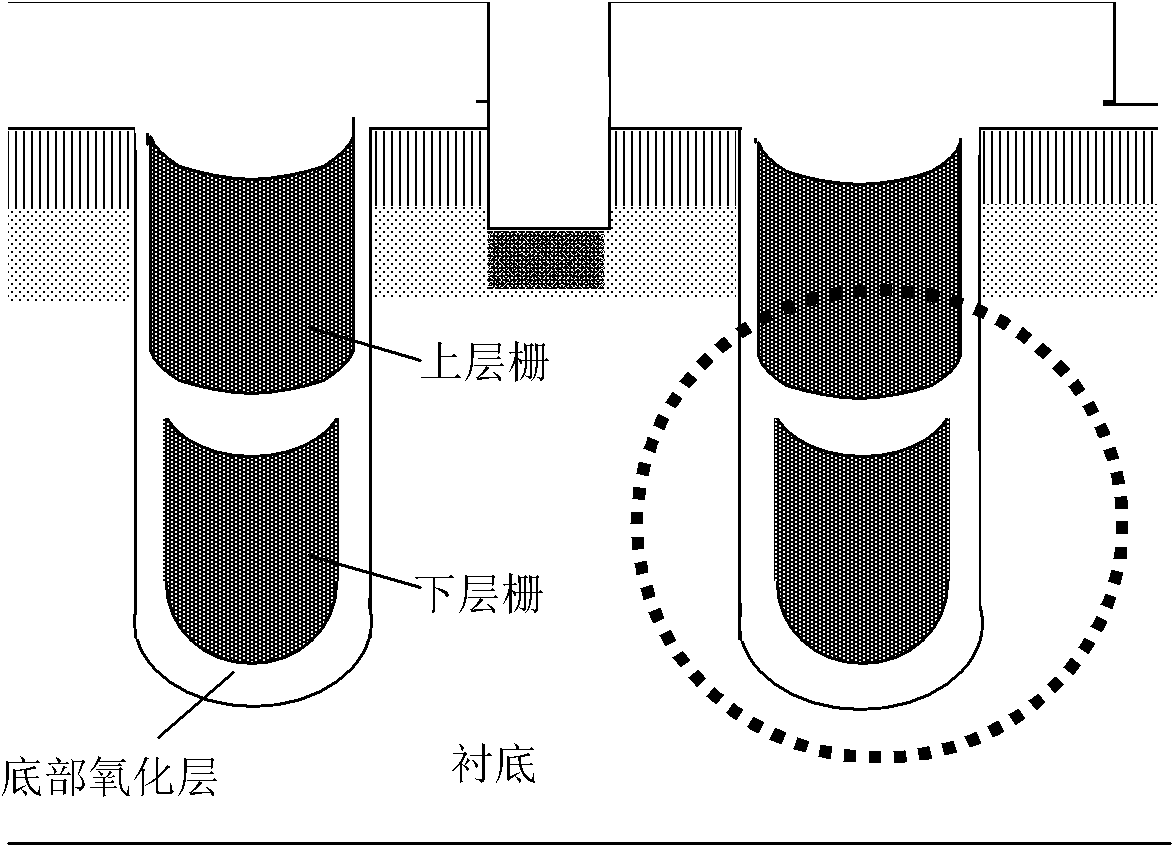
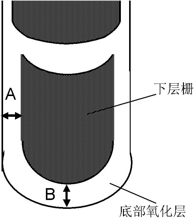
[0020] The method of the present invention is to reduce the source-drain capacitance through the thick bottom oxide layer on the existing double-layer gate trench MOS, and then effectively reduce its high-frequency operation on the basis of the original advantages of the double-layer gate trench MOS. under the power loss.

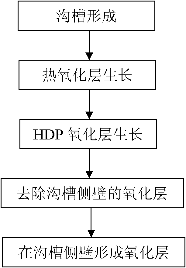
[0021] The method for forming the bottom oxide layer in the double-layer gate trench MOS structure of the present invention, see image 3 The process is described in detail below.

[0022] After trench formation (see Figure 5 ), first grow an oxide layer on the inner wall of the trench and the surface of the substrate, usually by thermal oxygen oxidation (see Image 6 ). The trench is etched using a conventional dry etching process. The depth and width of the trench are the same or similar to those of the existing double-layer gate trench MOS device. The thermal oxide layer is grown by using a thermal oxygen process to oxidize silicon to form an oxide...


PUM


Abstract

The invention relates to a method for forming a bottom oxide layer in a double-layered gate groove MOS (Metal Oxide Semiconductor) structure. The method comprises the following steps: 1) after a groove is formed, growing an oxide layer on an inner wall of a groove and the surface of a substrate; 2) depositing the oxide layer by adopting a HDP (High Density Plasma) technique, and forming a HDP oxide layer with preset thickness in the groove; 3) removing the oxide layer positioned at the side wall of the groove; and 4) forming the oxide layer on the side wall of the groove, so that the preparation of the bottom oxide layer in the double-layered gate groove MOS structure can be finished. According to the method disclosed by the invention, the structure with the thicker bottom oxide layer is formed and capacitance between the source electrode and the drain electrode of a device is efficiently reduced.

Description

technical field [0001] The invention relates to a preparation method of a double-layer gate trench MOS structure, in particular to a preparation method of a bottom oxide layer in the double-layer gate trench MOS structure. Background technique [0002] The current mainstream double-layer gate trench MOS structure, see figure 1 As shown, there are two polysilicon gates in the trench, the lower gate is a shield gate, the upper gate is a control gate, and the two gates are insulated from each other. When connecting the shielded gate to the source, the shielded gate can also be called source polysilicon (source poly), and the control gate controls the channel of the MOS device. In the existing double-layer gate trench MOS structure, the oxide layer (see figure 2 area A) and the bottom oxide layer (see figure 2 area B) of the same thickness. The shielding gate is between the control gate and the drain to act as a shield, so that the control gate-drain capacitance is reduced...

Claims


Application Information

Patent Timeline
IPC IPC(8): H01L21/336H01L21/316
Inventor 李陆萍丛茂杰金勤海
Owner SHANGHAI HUAHONG GRACE SEMICON MFG CORP
Why Eureka
Try Eureka