Tunneling field effect transistor structure with suspended source and drain regions and forming method thereof

A tunneling field effect and transistor technology, which is applied in semiconductor devices, semiconductor/solid-state device manufacturing, electrical components, etc., can solve the problems of increased delay in digital circuits, reduce source-drain capacitance, suppress off-state leakage, The effect of improving work speed

Active Publication Date: 2013-07-31
TSINGHUA UNIV
View PDF3 Cites 0 Cited by
  • Summary
  • Abstract
  • Description
  • Claims
  • Application Information

AI Technical Summary

Problems solved by technology

[0006] The disadvantage of the existing technology is that the performance of TFET devices needs to be improved, especially the delay of digital circuits caused by source-drain capacitance

Method used


Image

  • Tunneling field effect transistor structure with suspended source and drain regions and forming method thereof
  • Tunneling field effect transistor structure with suspended source and drain regions and forming method thereof
  • Tunneling field effect transistor structure with suspended source and drain regions and forming method thereof

Examples


Embodiment Construction

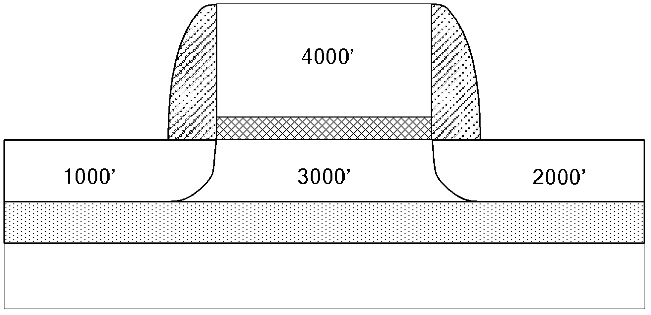
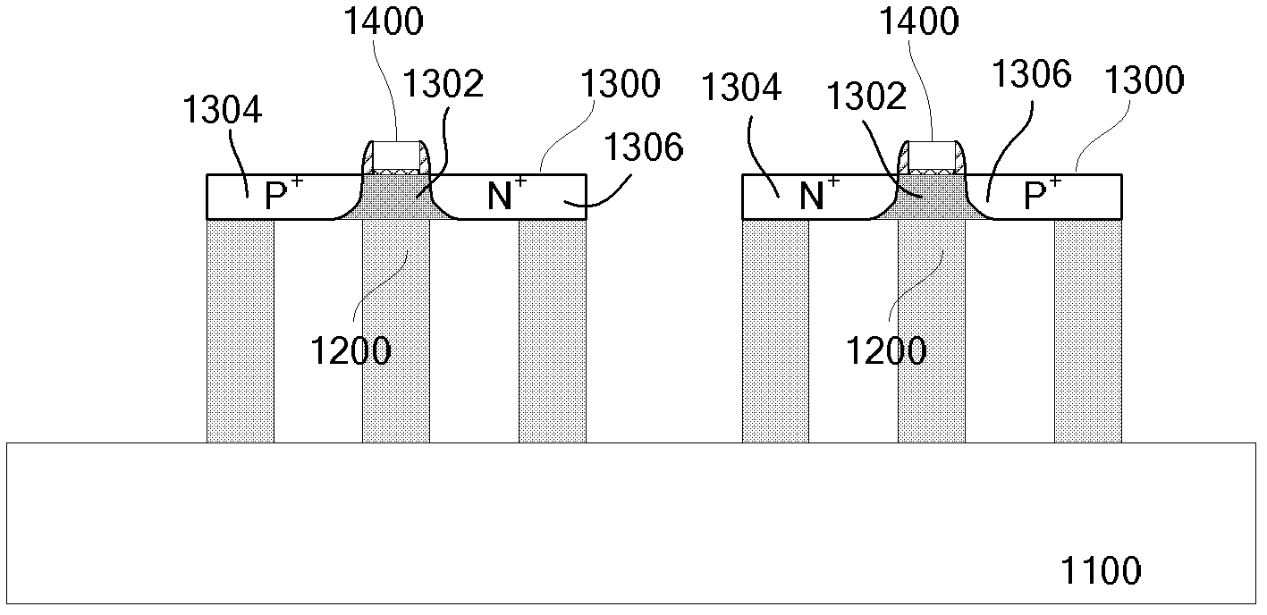
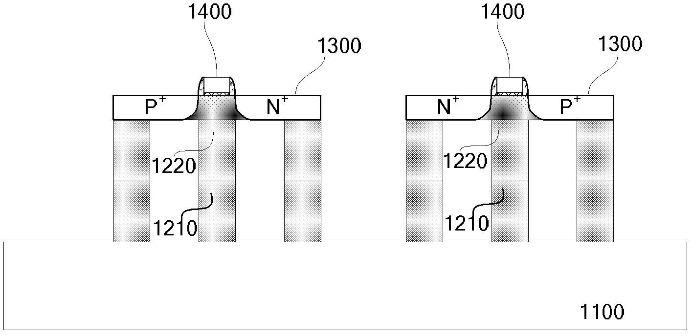
[0038] The following describes in detail the embodiments of the present invention, examples of which are illustrated in the accompanying drawings, wherein the same or similar reference numerals refer to the same or similar elements or elements having the same or similar functions throughout. The embodiments described below with reference to the accompanying drawings are exemplary and are only used to explain the present invention, but not to be construed as a limitation of the present invention.

[0039] The following disclosure provides many different embodiments or examples for implementing different structures of the invention. In order to simplify the disclosure of the present invention, the components and arrangements of specific examples are described below. Of course, they are only examples and are not intended to limit the invention. Furthermore, the present invention may repeat reference numerals and / or letters in different instances. This repetition is for the purp...


PUM


Abstract

Provided are a tunneling field effect transistor structure and a forming method thereof. The tunneling field effect transistor structure includes: a substrate (1100); a plurality of bulge structures (1200) formed on the substrate (1100), wherein there is a certain gap between each two bulge structures (1200), and the plurality of bulge structures (1200) include a plurality of groups, each group includes at least two bulge structures (1200); a plurality of suspending layers (1300) formed on the bulge structures (1200) and corresponding to each group of bulge structures (1200) one by one respectively, wherein the suspending layer (1300) region corresponding to the top of the intermediate bulge structure (1200) in each group of bulge structures (1200) is formed as a channel area (1302), and the suspending layer (1300) region on either side of the channel area (1302) is formed as a source area (1304) and a drain area (1306) with opposite conductive types respectively; and a gate stack (1400) formed at the top of the channel area (1302).

Description

technical field [0001] The invention relates to the technical field of semiconductor design and manufacture, in particular to a structure of a tunneling field effect transistor with floating source and drain and a forming method thereof. Background technique [0002] For a long time, in order to obtain higher chip density, faster working speed and lower power consumption. The feature size of Metal-Oxide-Semiconductor Field Effect Transistors (MOSFETs) has been shrinking continuously following the so-called Moore's law, and their operating speeds are getting faster and faster. At present, it has entered the range of nanoscale. However, a serious challenge that comes with it is the appearance of short-channel effects, such as subthreshold voltage drop (Vt roll-off), drain-induced barrier lowering (DIBL), and source-drain punch through (punch through), etc. , making the off-state leakage current of the device significantly increased, resulting in performance degradation. [...

Claims


Application Information

Patent Timeline
Patent Type & Authority Patents(China)
IPC IPC(8): H01L29/78H01L29/10H01L21/336
CPCH01L29/0657H01L29/10H01L29/7391H01L29/78
Inventor 崔宁梁仁荣王敬许军
Owner TSINGHUA UNIV
Why Eureka
Try Eureka