
Nonvolatile memory unit and memory

A non-volatile storage and storage unit technology, applied in static memory, digital memory information, information storage, etc., can solve problems such as unfavorable three-dimensional high-density integration of non-volatile memory, and achieve the effect of realizing rectification characteristics

Active Publication Date: 2014-02-12
INST OF MICROELECTRONICS CHINESE ACAD OF SCI
View PDF3 Cites 0 Cited by
  • Summary
  • Abstract
  • Description
  • Claims
  • Application Information

AI Technical Summary

Problems solved by technology

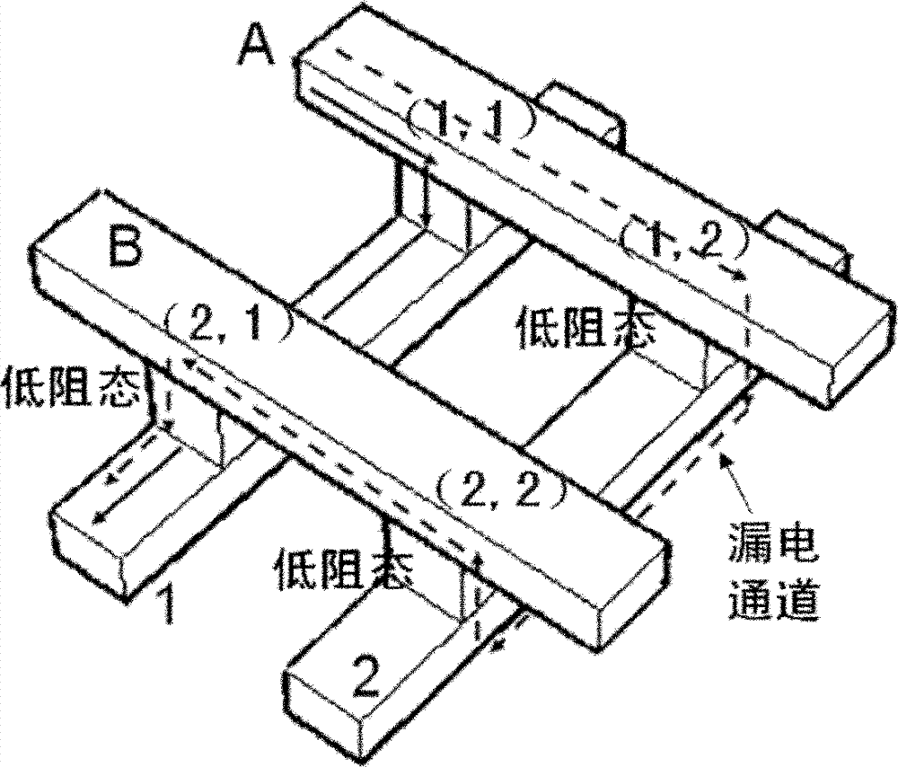
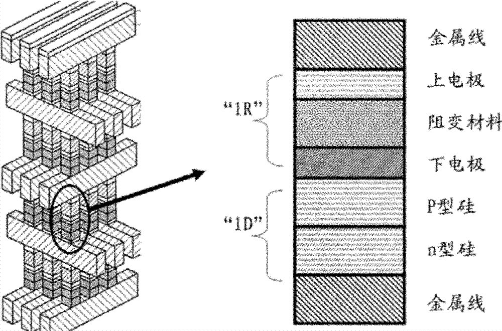
[0007] In the process of realizing the present invention, the inventor realized that there are the following technical problems in the prior art: in the resistive memory cell with 1D1R structure using PN junction as the gate unit, due to the need for additional doping and high-temperature activation process, there is no Facilitate 3D high-density integration of non-volatile memories

Method used


Image

  • Nonvolatile memory unit and memory
  • Nonvolatile memory unit and memory
  • Nonvolatile memory unit and memory

Examples


Embodiment Construction

[0030] In order to make the object, technical solution and advantages of the present invention clearer, the present invention will be described in further detail below in conjunction with specific embodiments and with reference to the accompanying drawings.

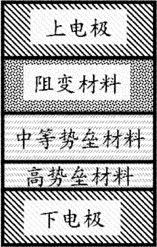
[0031]In an exemplary embodiment of the present invention, a non-volatile memory unit is provided. The storage unit includes: an upper electrode, a gate function layer, a resistance switching function layer and a lower electrode, and the upper electrode and the lower electrode are formed at two ends of the storage unit. The gating functional layer alone or together with the resistive switching functional layer forms an asymmetric tunneling barrier structure. The asymmetric tunnel barrier structure is used to realize the rectification and modulation of the forward and reverse tunneling current passing through the non-volatile storage unit. Preferably, the barrier heights of the materials constituting the asymmetric tunnel...


PUM


Abstract

A nonvolatile memory unit and a memory device are provided. The memory unit includes an upper electrode (1), a dissymmetrical tunnel barrier structure and a lower electrode (5) in turn from top to bottom, wherein the dissymmetrical tunnel barrier structure is applied to achieve rectifier modulation for forward and reverse tunnel current through the nonvolatile memory unit. The memory unit is applied different polarity voltage on both sides of the dissymmetrical barrier, so as to modulate the tunnel current by adjusting height of dissymmetrical barrier and thickness of tunnel, to obtain large difference of forward and reverse current; and thus achieve rectification character effectively.

Description

technical field [0001] The invention belongs to the technical field of microelectronics and memory, and in particular relates to a non-volatile memory unit and memory for high-density data storage. Background technique [0002] Resistive random access memory (resistive random access memory, referred to as RRAM), as an emerging non-volatile storage technology, has great advantages in terms of cell area, device density, power consumption, programming / erasing speed, 3D integration and multi-value implementation, etc. Compared with FLASH, it has great advantages in many aspects, and has been highly concerned by large companies and research institutes at home and abroad. The continuous progress of resistive memory technology makes it one of the most powerful competitors for mainstream products in the future non-volatile memory technology market. [0003] Resistive memory has a simple cell structure of electrode / insulating layer / electrode. Therefore, the 1R cross-array structure ...

Claims


Application Information

Patent Timeline
Patent Type & Authority Patents(China)
IPC IPC(8): H01L45/00
CPCH01L27/2481G11C2213/72G11C13/0007G11C2213/73H01L45/145G11C2213/54H01L45/04G11C2013/0073G11C13/003H10B63/84H10N70/20H10N70/883
Inventor 霍宗亮刘明刘璟王艳花龙世兵
Owner INST OF MICROELECTRONICS CHINESE ACAD OF SCI
Learn More