Preparation method of MOS transistor

A technology of MOS transistors and manufacturing methods, applied in semiconductor/solid-state device manufacturing, electrical components, circuits, etc., can solve the problems of increased electrical activation junction leakage, low junction leakage performance, and large junction leakage, etc., to reduce junction leakage, The effect of good electrical characteristics

Active Publication Date: 2012-08-01
SEMICON MFG INT (SHANGHAI) CORP
View PDF5 Cites 12 Cited by
  • Summary
  • Abstract
  • Description
  • Claims
  • Application Information

AI Technical Summary

Problems solved by technology

When this method uses Ge ion implantation to eliminate the short channel effect caused by As ion implantation, it is easy to produce transient enhanced diffusion effect (TED), resulting in the degradation of short channel device characteristics and greater junction leakage; C ion implantation eliminates Ge as an important component. The defects caused by ion implantation will degrade the electrical activation of As ions and cause increased junction leakage (hot carrier injection effect, HCI), so the ultra-shallow junction formed by this method is still difficult to achieve SCE (short channel effect ) and RSCE (reverse short channel effect) control and lower junction leakage performance

Method used


Image

  • Preparation method of MOS transistor
  • Preparation method of MOS transistor
  • Preparation method of MOS transistor

Examples


Embodiment Construction

[0025] The manufacturing method of the MOS transistor proposed by the present invention will be further described in detail below with reference to the drawings and specific embodiments. Advantages and features of the present invention will be apparent from the following description and claims. It should be noted that all the drawings are in very simplified form, and are only used for the purpose of conveniently and clearly assisting in describing the embodiments of the present invention.

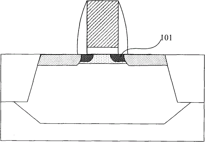
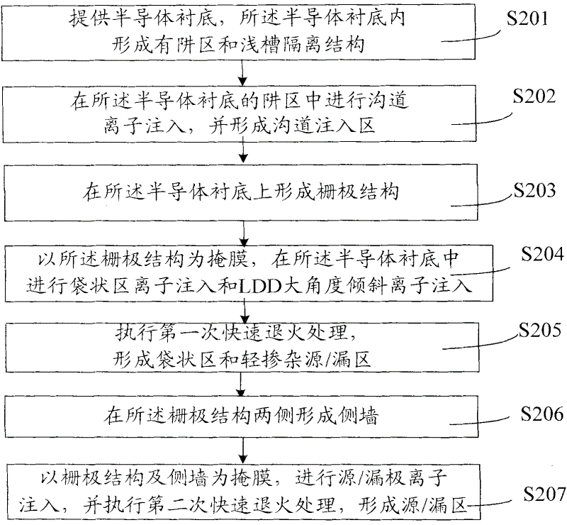
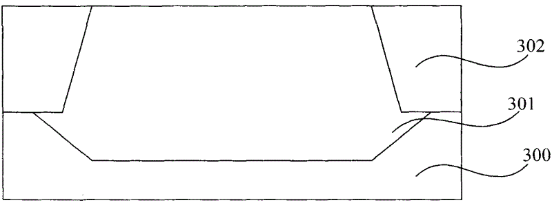
[0026] Such as figure 2 As shown, the present invention provides a method for manufacturing a MOS transistor, which is completed by six steps from S201 to S206, combined below figure 2 The flow chart of the fabrication process of the MOS transistor and Figure 3A-3G The schematic cross-sectional structural diagram of the manufacturing process of the MOS transistor is described in detail for the manufacturing method of the above-mentioned MOS transistor.

[0027] S201. A semiconductor s...


PUM


Abstract

The invention provides a preparation method of an MOS transistor, comprising: providing a semiconductor substrate, wherein a well region and a shallow-slot isolation structure are formed in the semiconductor substrate; carrying outchannel ion injection in the well region of the semiconductor substrate to form a channel injection region; forming a grid structure on the semiconductor substrate; carrying out a bag-like region ion injection and a lightly doped source/drain region(LDD) large angle inclined ion injection, wherein the grid structure is used as a mask; carrying out a first rapid thermal annealing process to form the bag-like region and the lightly doped source/drain region; forming side walls on two sides of the grid structure; and carrying out a source/drain ion injection and a second rapid thermal annealing process to form source/drain regions, wherein the grid structure and the side walls are used as masks. According to the preparation method of the invention, an ultra-shallow junction MOS transistor with longer effective channels is formed through the LDD large angle inclined ion injection. Thus, HCI effects can be inhibited, SCE effects can be substantially improved, and junction electric leakage can be decreased.

Description

technical field [0001] The invention relates to the field of semiconductor manufacturing, in particular to a method for manufacturing a MOS transistor. Background technique [0002] With the advancement of the semiconductor industry, the feature size and depth of semiconductor devices continue to shrink, especially when entering the node of 65 nanometers and below, requiring the source / drain region and the source / drain extension region (Source / DrainExtension) to become shallower accordingly, and the junction The doped junction with a depth below 100nm is usually called an ultra-shallow junction (USJ). The ultra-shallow junction can better improve the short-channel effect of the device, but with the further improvement of the device size and performance, the junction leakage phenomenon is a super-shallow junction. Shallow knot technology increasingly needs to solve problems. [0003] In the prior art, As, Ge, and C ions are usually implanted in sequence to form a lightly dop...

Claims


Application Information

Patent Timeline
Patent Type & Authority Applications(China)
IPC IPC(8): H01L21/336H01L21/266
CPCH01L29/6659
Inventor 赵猛
Owner SEMICON MFG INT (SHANGHAI) CORP
Why Eureka
Try Eureka