Chip scale package (CSP) chip mounting loading device and mounting method

A chip mounting and carrier technology, which is applied to the assembly of printed circuits with electrical components, electrical components, semiconductor/solid-state device manufacturing, etc., can solve the problems of accumulative errors that cannot be produced in multiple chips, high equipment costs, etc., and improve the welding yield. and straight-through rate, optimize the mass production process, and reduce the effect of equipment investment cost

Active Publication Date: 2012-08-01
SUZHOU ETRON TECH CO LTD
View PDF4 Cites 8 Cited by
  • Summary
  • Abstract
  • Description
  • Claims
  • Application Information

AI Technical Summary

Problems solved by technology

The existing CSP chip flip-chip technology must use semiconductor-level assembly equipment, and the equipment cost is relatively high. In addition, because the pad diameter and spacing of the CSP chip are ultra-small, the design of the carrier board is a precision and semiconductor design. In order to improve the Product quality, usually a single-chip carrier board is produced, and the placement operation requires mass production, and the single-chip is arranged in multiple pieces, which will cause cumulative errors and make it impossible to carry out multi-chip production

Method used


Image

  • Chip scale package (CSP) chip mounting loading device and mounting method
  • Chip scale package (CSP) chip mounting loading device and mounting method

Examples


Embodiment Construction

[0020] The specific implementation manners of the present invention will be further described in detail below in conjunction with the accompanying drawings and embodiments. The following examples are used to illustrate the present invention, but are not intended to limit the scope of the present invention.

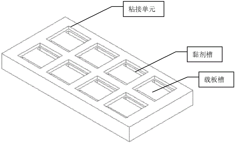
[0021] Such as figure 1 As shown, the CSP die-attaching carrier described in the present invention is provided with a plurality of bonding units on the carrier, and the bonding unit includes a carrier groove for placing a carrier to be mounted, and a Adhesive groove on the edge of the carrier board groove to be mounted, where the adhesive used to stick the carrier board to be mounted is placed.

[0022] The carrier and the bonding unit are rectangular.

[0023] The bonding units are arranged symmetrically with respect to the perpendicular to the opposite sides of the rectangle formed by the carrier.

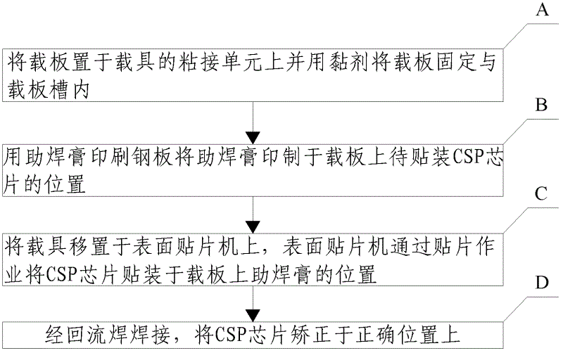
[0024] Such as figure 2 As shown, the method for mounting the CSP c...


PUM


Abstract

The invention discloses a chip scale package (CSP) chip mounting supporting device and a mounting method, and relates to the technical field of semiconductor assembly. The supporting device is provided with a plurality of adhesive units, and the adhesive units comprise supporting plate grooves for placing supporting plates to be mounted and adhesive grooves located on the edges of the grooves of the supporting plates to be mounted and used for placing adhesive for adhering with the supporting plates to be mounted. CSP chips are mounted on the chip supporting plates by using a traditional surface mounting technology (SMT) surface mounting device, and no semiconductor level special assembly device is needed, so that investment cost of the device is reduced. The CSP chip mounting supporting device achieves multi-chip layout arrangement of the supporting plates, optimizes mass production processes of CSP chip mounting, reduces part accumulative errors, simultaneously can assemble the CSP chips effectively and rapidly, and improves welding yield and rolled yield of products.

Description

technical field [0001] The invention relates to the technical field of semiconductor assembly, in particular to a CSP chip mount carrier and a mount method. Background technique [0002] In recent years, the application of consumer electronic products such as mobile phones, digital cameras, tablet computers, ultra-thin notebook computers and thin displays has penetrated into various fields of life. The demand for consumer electronic products is also gradually changing towards thinner and smaller, so more and more components of CSP integrated circuits are used in consumer electronic products. [0003] The traditional CSP chip assembly method usually uses a pad diameter of 0.35mm and a center spacing of 0.500mm as the demarcation point between the traditional SMT surface mount industry and the semiconductor-level assembly industry; the size larger than this boundary line usually belongs to the traditional SMT surface The processing of the patch, which is smaller than this bou...

Claims


Application Information

Patent Timeline
Patent Type & Authority Applications(China)
IPC IPC(8): H01L21/67H01L21/50H05K3/34
Inventor 钱新栋陈献祥
Owner SUZHOU ETRON TECH CO LTD
Why Eureka
Try Eureka