Eureka AIR delivers breakthrough ideas for toughest innovation challenges, trusted by R&D personnel around the world.

Low-voltage differential signaling transmitter

A low-voltage differential signal and transmitter technology, applied in the field of data transmission, can solve the problems of small voltage division, LVDS transmitter performance degradation, entering the linear region, etc.

Active Publication Date: 2012-08-01
HUAWEI TECH CO LTD
View PDF4 Cites 15 Cited by
  • Summary
  • Abstract
  • Description
  • Claims
  • Application Information

AI Technical Summary

Problems solved by technology

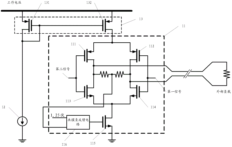
[0006] Embodiments of the present invention provide a low-voltage differential signal LVDS transmitter, which can solve the problem in the prior art that due to the low operating voltage, the divided voltage obtained by the fourth PMOS is small and enters the linear region, resulting in the performance of the LVDS transmitter. Deterioration problem

Method used


Image

  • Low-voltage differential signaling transmitter
  • Low-voltage differential signaling transmitter
  • Low-voltage differential signaling transmitter

Examples


Embodiment Construction

[0020] The following will clearly and completely describe the technical solutions in the embodiments of the present invention with reference to the accompanying drawings in the embodiments of the present invention. Obviously, the described embodiments are only some, not all, embodiments of the present invention. Based on the embodiments of the present invention, all other embodiments obtained by persons of ordinary skill in the art without creative efforts fall within the protection scope of the present invention.

[0021] In order to make the advantages of the technical solution of the present invention clearer, the present invention will be described in detail below in conjunction with the accompanying drawings and embodiments.

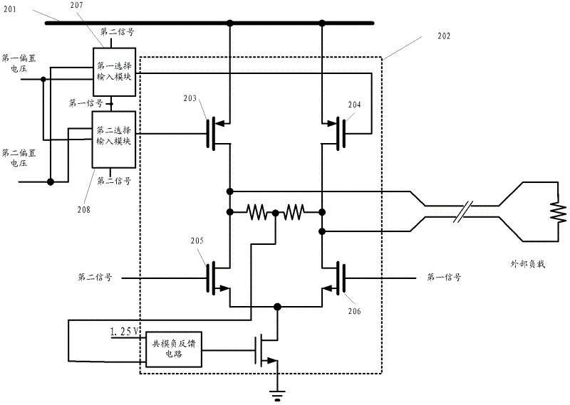
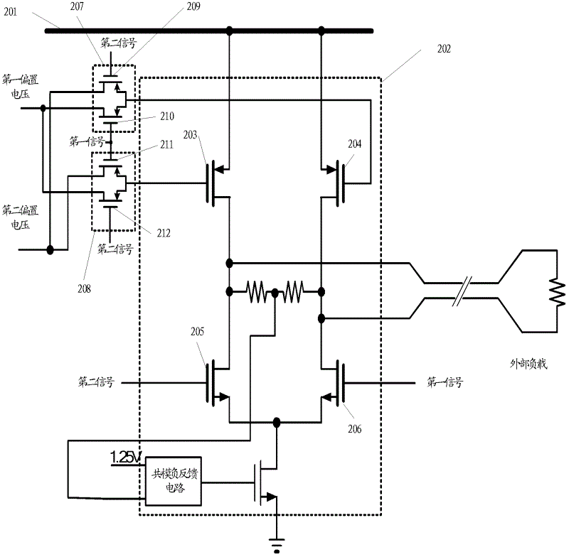
[0022] Such as figure 2 As shown, the low-voltage differential signal LVDS transmitter provided by the embodiment of the present invention includes a working power supply 201 and a transmitter main body 202, and the transmitter main body 202 includ...


PUM


Abstract

The embodiment of the invention discloses a low-voltage differential signaling (LVDS) transmitter, which relates to the technical field of data transmission and solves the problem that the performance of the LVDS transmitter in the prior art is degraded. The transmitter comprises a working power supply, a main transmitter part, a first selective input module and a second selective input module, the main transmitter part comprises a first PMOS (P-channel Metal Oxide Semiconductor) transistor, a second PMOS transistor, a first NMOS (N-channel Metal Oxide Semiconductor) transistor and a second NMOS transistor, and the sources of the first PMOS transistor and the second PMOS transistor are connected with the working power supply; both the first selective input module and the second selective input module are loaded with a first signal, a second signal, first bias voltage and second bias voltage, the first bias voltage or the second bias voltage is selectively inputted into the grids of the first PMOS transistor and the second PMOS transistor according to the first signal and the second signal, the voltage loaded into the grid of the first PMOS transistor is different from the voltage loaded into the grid of the second PMOS transistor in real time, and the first signal and the second signal are a pair of different-mode signals in order to carry out the function of the LVDS transmitter.

Description

technical field [0001] The invention relates to the technical field of data transmission, in particular to a low-voltage differential signal transmitter. Background technique [0002] Low Voltage Differential Signaling (LVDS for short) is widely used in short-distance interconnection between chips. The communication system of the LVDS signal usually includes an LVDS transmitter, and the LVDS transmitter is used for converting the working level in the chip into an LVDS signal and sending the LVDS signal out. [0003] A prior art LVDS transmitter such as figure 1 As shown, the LVDS transmitter includes a transmitter main body 11, a current source 12, and a P-type metal oxide semiconductor (Positive channel Metal Oxide Semiconductor, PMOS for short) connected to the current source 12 and the transmitter main body 11. ) tube current mirror 13, the PMOS tube current mirror includes a third PMOS tube 131 and a fourth PMOS tube 132, the current source 12 generates a current (gene...

Claims


Application Information

Patent Timeline
Patent Type & Authority Applications(China)
IPC IPC(8): H04L25/02H03K19/0185
Inventor 杨奕
Owner HUAWEI TECH CO LTD
Why Eureka
Eureka Blog
Learn More