Array substrate, manufacturing method of array substrate and liquid crystal display device

A technology of an array substrate and a manufacturing method, applied in the field of liquid crystal display, can solve the problems of reducing the area and reducing the pixel aperture ratio, and achieve the effects of increasing the area, improving the pixel aperture ratio, and reducing the capacitance effect.

Active Publication Date: 2015-05-20
BEIJING BOE OPTOELECTRONCIS TECH CO LTD
View PDF4 Cites 1 Cited by
  • Summary
  • Abstract
  • Description
  • Claims
  • Application Information

AI Technical Summary

Problems solved by technology

In order to reduce the capacitive effect, the pixel electrode and the data line are generally designed to be farther apart, but this reduces the area occupied by the pixel electrode and reduces the pixel aperture ratio.

Method used


Image

  • Array substrate, manufacturing method of array substrate and liquid crystal display device
  • Array substrate, manufacturing method of array substrate and liquid crystal display device
  • Array substrate, manufacturing method of array substrate and liquid crystal display device

Examples


Embodiment Construction

[0030] The array substrate, its manufacturing method, and liquid crystal display device according to the embodiments of the present invention will be described in detail below with reference to the accompanying drawings.

[0031] It should be clear that the described embodiments are only some of the embodiments of the present invention, not all of them. Based on the embodiments of the present invention, all other embodiments obtained by persons of ordinary skill in the art without creative efforts fall within the protection scope of the present invention.

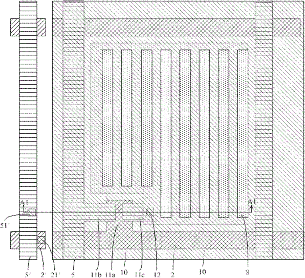
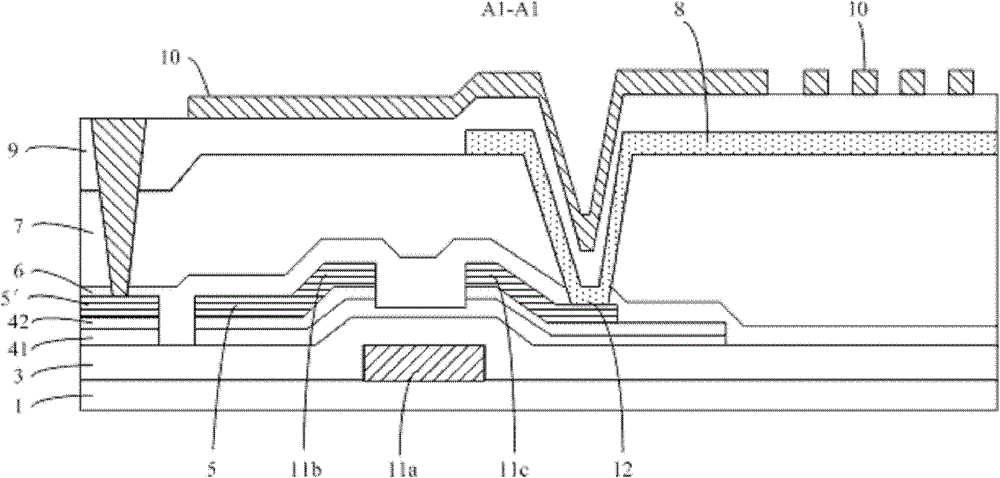
[0032] An embodiment of the present invention provides an array substrate, the following refers to figure 1 and Figure 1a The structure of the array substrate in this embodiment will be described. in, figure 1 Shown is a schematic plan view of the array substrate of the embodiment of the present invention; Figure 1a shown as figure 1 The cross-sectional view of the A1-A1 direction in the middle. The array substrate ...


PUM

PropertyMeasurementUnit
thicknessaaaaaaaaaa
thicknessaaaaaaaaaa
thicknessaaaaaaaaaa

Abstract

The invention discloses an array substrate, a manufacturing method of the array substrate and a liquid crystal display device, relates to the technical field of liquid crystal display and is invented for improving the pixel aperture ratio. The array substrate comprises a substrate; grid lines are arranged on the substrate; data lines are arranged vertically to the grid lines; pixel regions are defined between the grid lines and the data lines; thin film transistors and pixel electrodes are arranged in the pixel regions; grid electrodes of the thin film transistors are connected with the grid lines; source electrodes of the thin film transistors are connected with the data lines; drain electrodes of the thin film transistors are connected with the pixel electrodes; and a resin dielectric layer is arranged between the layer on which the pixel electrodes are positioned and the layer on which the data lines are positioned. The array substrate and the liquid crystal display device can be used for carrying out liquid crystal display.

Description

technical field [0001] The invention relates to the technical field of liquid crystal display, in particular to an array substrate, a manufacturing method thereof, and a liquid crystal display device. Background technique [0002] The liquid crystal panel of a thin film transistor liquid crystal display device includes an array substrate and a color filter substrate. In the manufacturing process of a thin film transistor liquid crystal display device, the array substrate and the color filter substrate can be separately manufactured, and then the array substrate and the color filter substrate are boxed and filled with liquid crystals. , to form a liquid crystal panel. Wherein, a gate line is provided on the array substrate, a data line is provided perpendicular to the gate line, a pixel area is defined between the gate line and the data line, and a thin film transistor and a pixel electrode are provided in the pixel area, The gate of the thin film transistor is connected to ...

Claims


Application Information

Patent Timeline
Patent Type & Authority Patents(China)
IPC IPC(8): G02F1/1362G02F1/1368H01L27/12H01L21/77
Inventor 郭建闵泰烨陈旭谢振宇张文余
Owner BEIJING BOE OPTOELECTRONCIS TECH CO LTD
Why Eureka
Try Eureka