Manufacturing method of array substrate, array substrate and liquid crystal display

A technology of an array substrate and a manufacturing method, which is applied in the field of liquid crystal displays, can solve the problems of poor TFT-LCD picture quality, movement, and poor friction lines, and achieve the effects of reducing the probability of failure, simplifying the process flow, and reducing production costs

Active Publication Date: 2012-08-08
BEIJING BOE OPTOELECTRONCIS TECH CO LTD
View PDF4 Cites 7 Cited by
  • Summary
  • Abstract
  • Description
  • Claims
  • Application Information

AI Technical Summary

Problems solved by technology

[0007] Since the patterns of each layer in the TFT-LCD array substrate are not the same, the array substrate formed in this way has a level difference. Therefore, when performing Rubbing treatment, there will often be rubbing mura defects.
Moreover, due to the level difference of the array substrate, the position of the support in the TFT-LCD will move, and may move to the display area, thus, bright or dark spots appear on the TFT-LCD
[0008] It can be seen that due to the level difference of the TFT-LCD array substrate, it is easy to cause poor picture quality of the TFT-LCD

Method used


Image

  • Manufacturing method of array substrate, array substrate and liquid crystal display
  • Manufacturing method of array substrate, array substrate and liquid crystal display
  • Manufacturing method of array substrate, array substrate and liquid crystal display

Examples


Embodiment Construction

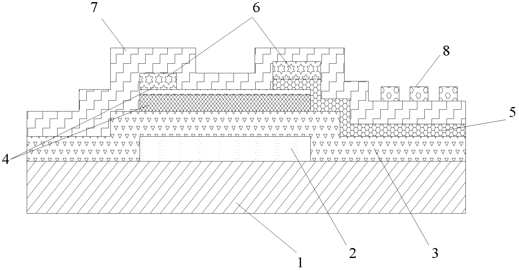
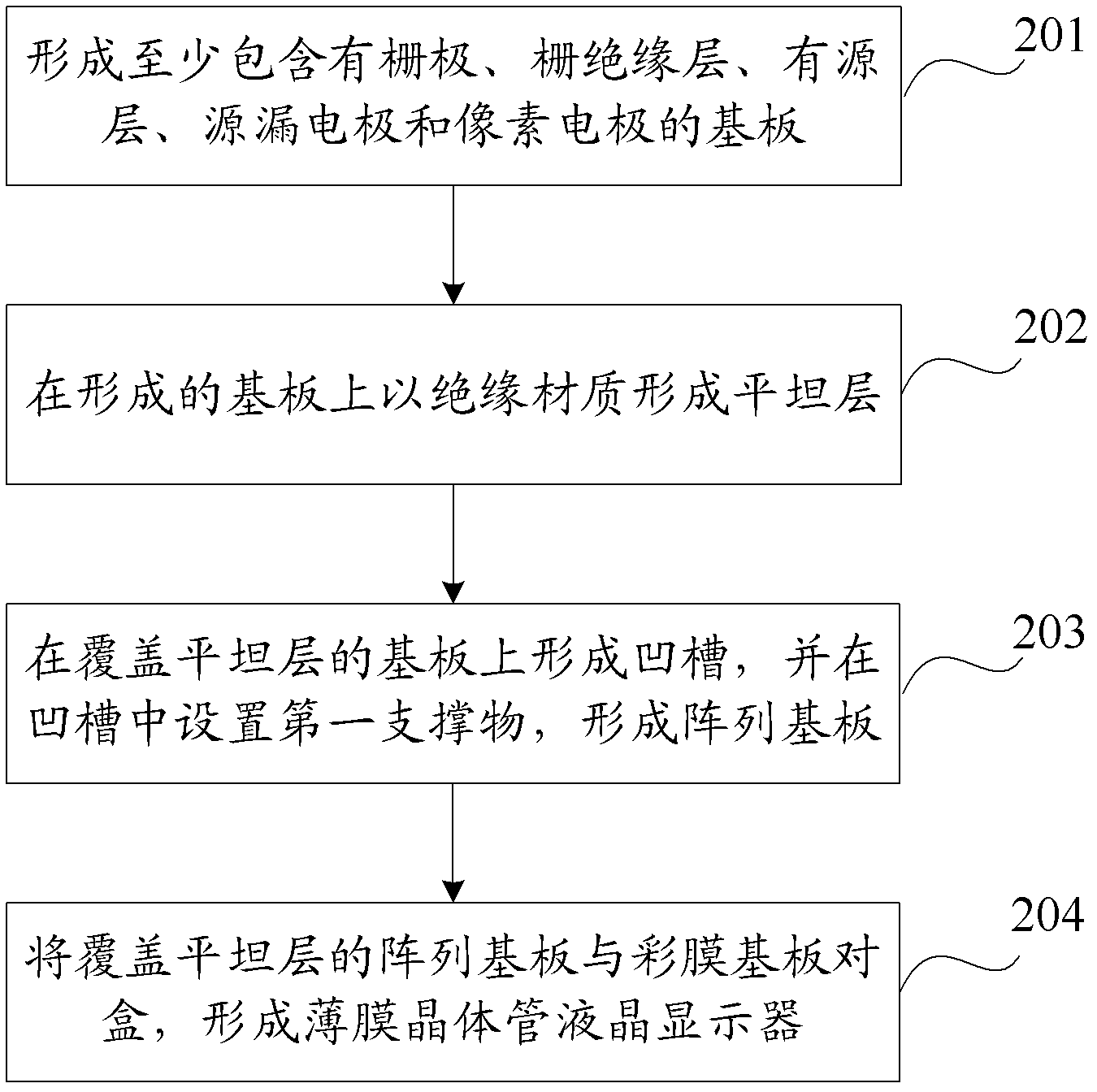
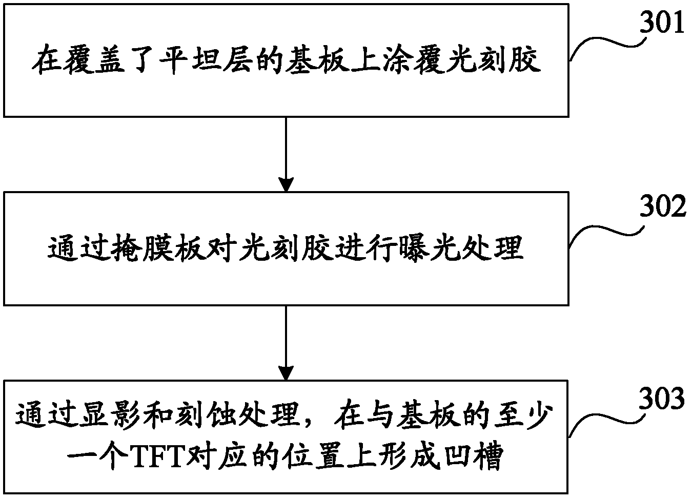
[0035] In an embodiment of the present invention, after forming a substrate including at least a gate, a gate insulating layer, an active layer, a source-drain electrode, and a pixel electrode, a planar layer is covered on the substrate, wherein the upper surface of the planar layer is a plane, Then, a groove is formed on the flat layer, and a first support is arranged in the groove, so that an array substrate is formed, and the array substrate and the color filter substrate are combined to form a thin film transistor liquid crystal display. In this way, since the upper surface of the flat layer is flat, the level difference caused by the different patterns of each layer of the array substrate is eliminated, and the chance of rubbing mura caused by the level difference is reduced, and there are grooves on the flat layer, which can reduce the movement of the support chance, improve the TFT-LCD picture quality.

[0036] see figure 2 , The process of TFT-LCD production includes...


PUM


Abstract

The invention discloses a manufacturing method of an array substrate, an array substrate and a liquid crystal display, thereby improving a picture quality of a thin film transistor liquid crystal display (TFT-LCD). The method comprises the following steps: forming a substrate at least containing a gate electrode, a gate insulation layer, an active layer, s source electrode, a drain electrode and a pixel electrode; forming a flat layer on the substrate; forming a groove on the flat layer; and arranging a first support in the groove.

Description

technical field [0001] The invention relates to the technical field of liquid crystal displays, in particular to a method for manufacturing an array substrate, an array substrate and a liquid crystal display. Background technique [0002] In recent years, with the advancement of science and technology, digital TV has begun to enter daily life. Thin Film Transistor Liquid Crystal Display (TFT-LCD) has become the current leading product due to its small size, low power consumption, and no radiation. [0003] TFT-LCD is formed by boxing the array substrate and the color filter substrate. In this way, the TFT-LC display forms an array of hundreds of thousands to millions of pixels, and each pixel displays images through the control of TFT. [0004] At present, the TFT-LCD array substrate is completed through multiple patterning processes, and each patterning process includes processes such as masking, exposure, development, etching, and stripping. The etching process includes d...

Claims


Application Information

Patent Timeline
Patent Type & Authority Applications(China)
IPC IPC(8): H01L21/77H01L27/02G02F1/1362G02F1/1368
Inventor 木素真
Owner BEIJING BOE OPTOELECTRONCIS TECH CO LTD
Why Eureka
Try Eureka