Conductive laminated body and touch panel using the same

A technology of conductive laminates and protective layers, applied in the field of conductive laminates, can solve the problems of slow processing speed, unsuitable for large-area processing, high cost, etc., and achieve good durability

Active Publication Date: 2012-08-08
TORAY IND INC
View PDF14 Cites 20 Cited by
  • Summary
  • Abstract
  • Description
  • Claims
  • Application Information

AI Technical Summary

Problems solved by technology

In the laser ablation method, since the conductive film is irradiated with a near-infrared (NIR) laser to remove unnecessary parts, it does not require a resist and can perform high-precision patterning. However, the applicable substrates are limited and the cost is high. , the processing speed is slow, so it is not suitable for large-area processing

Method used


Image

  • Conductive laminated body and touch panel using the same
  • Conductive laminated body and touch panel using the same
  • Conductive laminated body and touch panel using the same

Examples


Embodiment 1

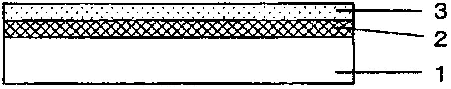
[0256] A polyethylene terephthalate film having a thickness of 125 μm, Lumiror (registered trademark) U46 (manufactured by Toray Corporation) was used as a base material, and “conductive layer A” was laminated on one surface of the base material.

[0257]Next, 296 g of "protective layer material A" and 704 g of "ethyl acetate" were mixed and stirred to prepare a protective layer coating liquid. Using a slot die coater equipped with a spacer made of sus (spacer thickness: 50 μm), apply this protective layer coating liquid on the above-mentioned “conductive layer A”, dry at 120° C. for 2 minutes, and set A protective layer having a thickness of 950 nm was used to obtain the conductive laminate of the present invention.

Embodiment 2

[0259] The composition of the protective layer coating solution was 500 g of "protective layer material A" and 1,500 g of "ethyl acetate". It was produced in the same manner as in Example 1, and a protective layer with a thickness of 800 nm was provided to obtain the conductive layer of the present invention. fit.

Embodiment 3

[0261] A polyethylene terephthalate film having a thickness of 125 μm, Lumiror (registered trademark) U46 (manufactured by Toray Corporation) was used as a base material, and “conductive layer B” was laminated on one surface of the base material.

[0262] Next, 150 g of "protective layer material B", 3.60 g of "additive A", 7.15 g of "additive B", and 1907 g of "ethyl acetate" were mixed and stirred to prepare a protective layer coating liquid. Using a slot die coater equipped with a spacer made of sus (spacer thickness: 50 μm), apply this protective layer coating solution on the above-mentioned "conductive layer B", and dry it at 120°C for 2 minutes. at 1.2J / cm 2 It cured by irradiating ultraviolet rays, provided a protective layer with a thickness of 450 nm, and obtained the conductive laminate of the present invention.


PUM

PropertyMeasurementUnit
thicknessaaaaaaaaaa
contact angleaaaaaaaaaa
thicknessaaaaaaaaaa

Abstract

Provided is a conductive laminated body which has resistance to removal agents employed in chemical etching performed when a conductive laminated body is processed to form an electrode member employed in a touch panel for example, and which has excellent durability with respect to heat. The conductive laminated body in which a conductive layer, which includes a conductive component having a network structure comprising a linear structure, and a protective layer are laminated from the substrate side on at least one face of the substrate, wherein the average thickness (t) of the protective layer is 100 to 1000 nm.

Description

technical field [0001] The present invention relates to a conductive laminate having a protective layer on a conductive layer containing a conductive component composed of a linear structure. More specifically, the present invention relates to a conductive laminate having resistance to a remover used in chemical etching when the conductive laminate is processed to form an electrode member used in a touch panel (touch panel) or the like, Good durability to heat. Furthermore, it relates to a conductive laminate that can also be used for electrode members used in display-related products such as liquid crystal displays, organic electroluminescence, and electronic paper, and solar cell modules. Background technique [0002] In recent years, mobile phones, game consoles, personal computers, and the like equipped with touch panels have spread. The conductive member for electrodes is used in the touch panel, and the conductive layer surface of the conductive member is formed into...

Claims


Application Information

Patent Timeline
Patent Type & Authority Applications(China)
IPC IPC(8): H01B5/14G06F3/045H01B13/00G06F3/041B32B7/02B32B27/18
CPCB32B7/02B32B27/18G06F2203/04103B32B15/08B32B27/20G06F3/041B32B15/02B32B2457/208Y10T428/265Y10T428/24744G06F3/044G06F3/045H01B5/14
Inventor 佐藤义和渡边修关口广树真多淳二
Owner TORAY IND INC
Why Eureka
Try Eureka