Display panel and method of manufacturing the same

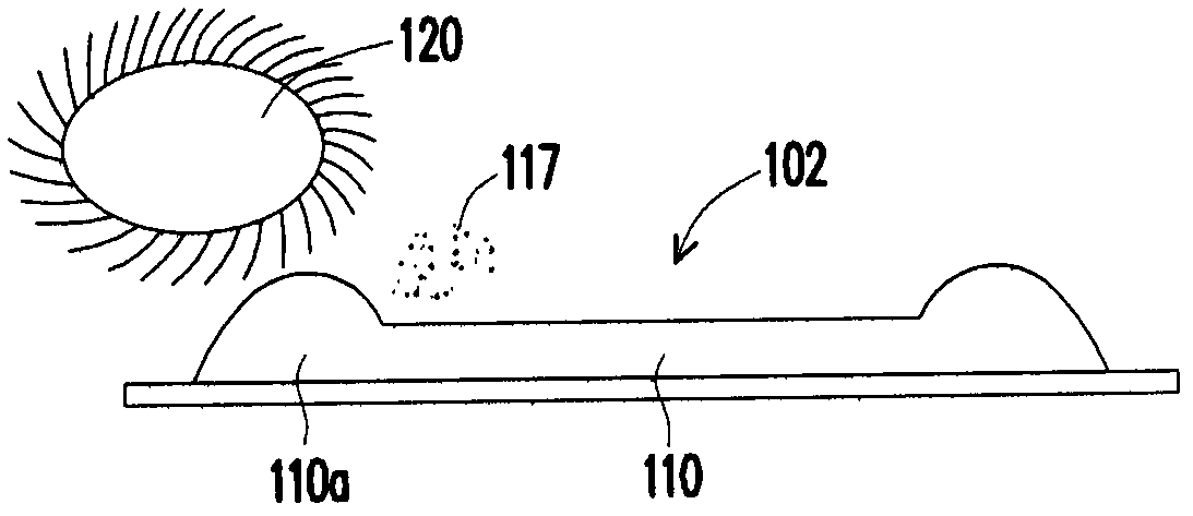
A technology for a display panel and a manufacturing method, applied in nonlinear optics, instruments, optics, etc., capable of solving problems such as debris 117 falling, affecting display quality, and uneven surface of an alignment material layer 110

Inactive Publication Date: 2012-08-15
AU OPTRONICS CORP
View PDF4 Cites 19 Cited by
  • Summary
  • Abstract
  • Description
  • Claims
  • Application Information

AI Technical Summary

Problems solved by technology

However, if figure 1 As shown, the alignment material layer 110 formed by the known technology for forming the alignment material layer 110 has the problem of uneven surface, for example, the edge of the alignment material layer 110 has a raised portion 110a
In this way, when the alignment pattern is

Method used


Image

  • Display panel and method of manufacturing the same
  • Display panel and method of manufacturing the same
  • Display panel and method of manufacturing the same

Examples


Embodiment Construction

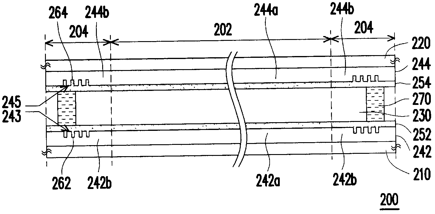
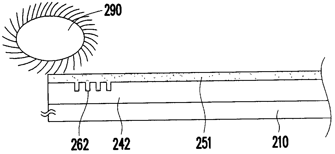
[0063] figure 2 It is a display panel according to an embodiment of the present invention. Such as figure 2 As shown, the display panel 200 includes a first substrate 210 , a second substrate 220 and a display medium 230 located between the first substrate 210 and the second substrate 220 . Here, the display medium 230 is, for example, a liquid crystal material, but the invention is not limited thereto. The first substrate 210 is, for example, an active device array substrate, and correspondingly, the second substrate 220 is, for example, a color filter substrate. In one embodiment, the first substrate 210 is, for example, a color filter substrate, and correspondingly, the second substrate 220 is, for example, an active device array substrate. Of course, in other embodiments, the first substrate 210 may also integrate an active element array substrate (Color Filter on Array, COA) with a color filter film, or an active element array substrate (Black matrix on Array) integr...


PUM


Abstract

The invention relates to a display panel and a method of manufacturing the same. The display panel is provided with a display area and a periphery area positioned thereoutside. The display panel comprises a first substrate, a first flat layer, a first alignment layer, a second substrate and a display medium. The first flat layer is arranged on the first substrate, and comprises a first portion positioned in the display area and a second portion positioned in the periphery area, wherein the top of the second portion is equipped with at least one first recess. The first alignment layer is disposed on the first flat layer, and a part of the first alignment layer is filled into the at least one first recess. The second substrate and the first substrate are arranged facing to each other. The display medium is arranged between the first substrate and the second substrate.

Description

technical field [0001] The present invention relates to a display panel and its manufacturing method, and in particular to a display panel suitable for adopting contact alignment technology and its manufacturing method. Background technique [0002] Liquid crystal displays have gradually become the mainstream of the market due to their superior characteristics such as high image quality, good space utilization efficiency, low power consumption, and no radiation. Wherein, in the manufacturing process of a specific liquid crystal display panel, such as an in-plane switching (IPS) liquid crystal display panel or a twisted nematic (twisted nematic) liquid crystal display panel, an alignment layer needs to be formed on the two substrates, To provide anchoring force to the liquid crystal molecules, so that the liquid crystal molecules are arranged in a specific direction. [0003] The existing method for forming an alignment layer is to align the alignment material after coating ...

Claims


Application Information

Patent Timeline
IPC IPC(8): G02F1/1337G02F1/1339G02F1/1333
Inventor 黄柏涵赵中立吴宜龙洪薏亘
Owner AU OPTRONICS CORP
Why Eureka
Try Eureka