Substrate processing device and substrate processing method

A technology for processing devices and substrates, which is applied to metal processing equipment, manufacturing tools, laser welding equipment, etc., and can solve problems such as decreased light extraction efficiency, rough surface roughness of split surfaces, and inability to obtain split sections.

Inactive Publication Date: 2012-08-29
MITSUBOSHI DIAMOND IND CO LTD
View PDF11 Cites 33 Cited by
  • Summary
  • Abstract
  • Description
  • Claims
  • Application Information

AI Technical Summary

Problems solved by technology

[0007] However, when processing a sapphire substrate made of a hard and brittle material by laser, regardless of the method of ablation or multiphoton absorption, the processing must increase the irradiation energy compared with glass processing, so when ablation is performed, the cutting groove The width of the groove becomes wider, and in the case of multiphoton absorption, the modified part inside the substrate becomes wider, and the surface roughness of the split surface formed by the modified part becomes rough, and it is impossible to obtain a high-precision split cross-section
Also, the light transmittance of the melted portion is impaired
Therefore, when a sapphire substrate is used as a substrate for a light-emitting element such as a light-emitting diode (LED), it becomes the main cause of a decrease in light extraction efficiency.

Method used


Image

  • Substrate processing device and substrate processing method
  • Substrate processing device and substrate processing method
  • Substrate processing device and substrate processing method

Examples


Embodiment Construction

[0068] Hereinafter, the board|substrate processing apparatus of this invention is demonstrated using drawing.

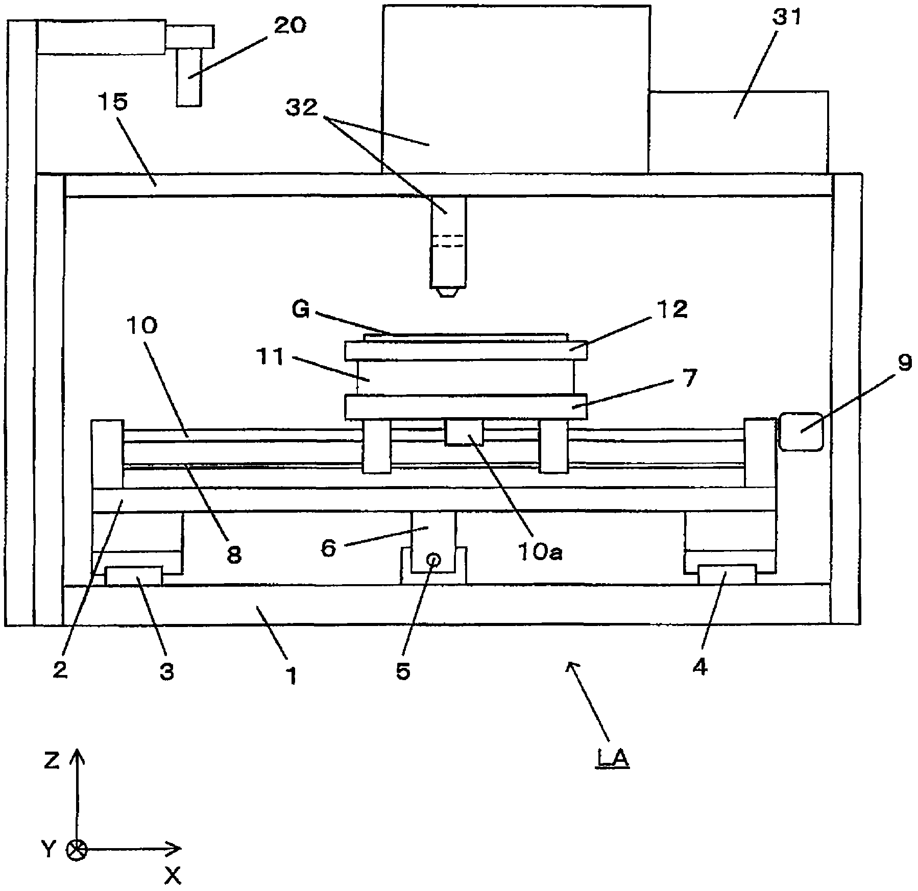
[0069] figure 1 It is an overall configuration diagram showing a substrate processing apparatus LA according to an embodiment of the present invention.

[0070] The substrate processing apparatus LA is configured such that a slide table 2 reciprocating in the front-rear direction of the drawing (hereinafter referred to as the Y direction) is provided along a pair of guide rails 3 and 4 arranged in parallel on the horizontal table 1 . Between the two guide rails 3 and 4, a screw 5 is arranged along the front and rear direction, and the stay bar 6 fixed on the slide table 2 is screwed to the screw 5, and the screw 5 is rotated by a motor (not shown), thereby sliding The table 2 moves in the Y direction along the guide rails 3 and 4 .

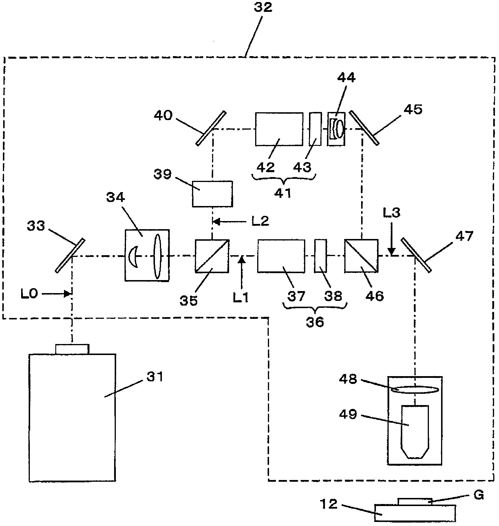
[0071] On the slide table 2, the horizontal platform base 7 is in the direction along the guide rail 8 figure 1 The left and right d...


PUM


Abstract

The invention provides a substrate processing device and a substrate processing method, which can conduct short pulse laser processing on the surface of the substrate and the internal part of the substrate without increasing scanning times. The substrate processing device comprises a short pulse laser light source (31), a light path branch part (35) which divide a short pulse laser beam into a first light path side and a second light path side, a pulse selection part (39) which converts repetitive oscillation frequency to make the second light path side to conduct repetitive oscillation of a second frequency smaller than the first frequency, an output adjustment part (36) which adjusts in a manner that the output power of the second light path side is larger than that of the first light path side, a light path synthesis part (46) which forms a synthetic laser beam by overlapping the first and second light path sides, a synthetic laser beam irradiation optical part (48) which comprises an object glass (49) and irradiates the synthetic laser beam towards the substrate, and a scanning mechanism which enables the synthetic laser beam to conduct relative scanning.

Description

technical field [0001] The present invention relates to a substrate processing device using a short-pulse laser, in particular to a substrate processing device and a substrate processing method suitable for processing a sapphire substrate as a hard and brittle material substrate. [0002] Herein, the so-called short pulse laser refers to the pulse width in 10 -13 ~10 -10 Second (0.1 ~ 100 picoseconds) of laser light. Background technique [0003] Several processing methods using pulsed lasers are known as processing methods for forming division starting points like dicing grooves (grooves) on brittle material substrates such as glass substrates, Si substrates, and sapphire substrates. What these processing methods have in common is that the substrate is heated by the energy irradiated with pulsed laser light, but the mechanism for forming the origin of division is quite different from each other, and each has different characteristics. [0004] For example, when breaking ...

Claims


Application Information

Patent Timeline
Patent Type & Authority Applications(China)
IPC IPC(8): B23K26/38B23K26/08B23K26/06B23K26/00B23K26/046B23K26/067B23K26/073B23K26/364H01L21/301
Inventor 中谷郁祥岩坪佑磨
Owner MITSUBOSHI DIAMOND IND CO LTD
Why Eureka
Try Eureka