Electroluminescent device, display device and preparation method of electroluminescent device

A technology for electroluminescent devices and light-emitting layers, which is applied in the fields of electro-solid devices, semiconductor/solid-state device manufacturing, electrical components, etc., can solve the problems of exciton quenching, low actual efficiency, and quantity mismatch, and improve the luminous efficiency. , the effect of increasing the compound ratio and prolonging the service life

Active Publication Date: 2012-08-29
BOE TECH GRP CO LTD
View PDF4 Cites 14 Cited by
  • Summary
  • Abstract
  • Description
  • Claims
  • Application Information

AI Technical Summary

Problems solved by technology

However, because the transport of carriers is not ideal, there may be uneven injection of carriers, and the injected carriers cannot recombine 100% to emit light, and the excitons formed by carrier recombination may even be quenched, which is Make the actual efficiency much lower than the maximum theoretical value
At the same time, when a voltage is applied on the light-emitting layer 103 through the anode layer 102 and the cathode layer 104, the mobility of the holes is higher than that of the electrons, but as the voltage increases, the growth rate of the mobility of the electrons will exceed that of the holes. The increase speed of the mobility of holes, so the position of the recombination region of the device will also change with the change of voltage, which will make the color of the device change significantly with the change of voltage
There are P-doped and N-doped devices, and the substrate that is conducive to electron transport is used to make the light-emitting layer. If it is a single recombination region, the light-emitting region should be closer to the hole-transport layer, which will also make the excess excitons Diffusion to the hole transport layer, no radiation attenuation, resulting in a mismatch in the number of carriers such as electrons and holes in the light-emitting layer 103, reducing the luminous efficiency of the light-emitting layer 103, which has an adverse effect on improving device efficiency

Method used


Image

  • Electroluminescent device, display device and preparation method of electroluminescent device
  • Electroluminescent device, display device and preparation method of electroluminescent device
  • Electroluminescent device, display device and preparation method of electroluminescent device

Examples


Embodiment Construction

[0036] In order to enable those skilled in the art to better understand the technical solution of the present invention, the electroluminescent device, the display device and the preparation method of the electroluminescent device provided by the present invention will be described in detail below with reference to the accompanying drawings.

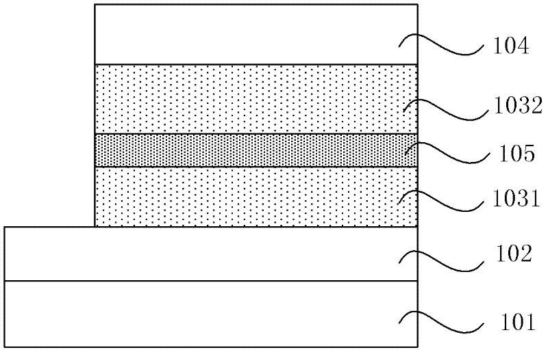
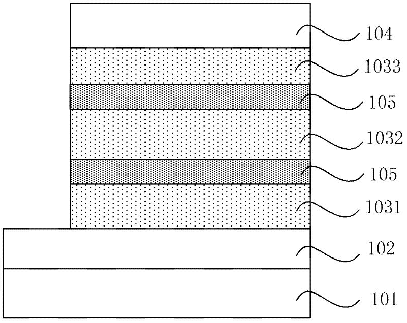
[0037] figure 2 It is a schematic structural diagram of the first embodiment of the electroluminescence device of the present invention. Such as figure 2 As shown, the electroluminescent device of this embodiment includes a substrate 101, an anode layer 102, a light emitting layer, and a cathode layer 104 in sequence, wherein the light emitting layer includes a first light emitting sublayer 1031 and a second light emitting sublayer 1032, and the first light emitting sublayer Between the layer 1031 and the second light-emitting sub-layer 1032 is provided an intercalation layer 105 which adjusts the transport of electrons to match the n...


PUM


Abstract

The invention provides an electroluminescent device, a display device and a preparation method of the electroluminescent device. The electroluminescent device sequentially comprises a substrate, an anode layer, a luminescent layer and a cathode layer, wherein the anode layer and the cathode layer are respectively connected with the anode and the cathode of a power supply. The electroluminescent device also comprises an inert layer for adjusting electron mobility, and the insert layer is arranged inside the luminescent layer. According to the embodiment of the invention, the insert layer is arranged inside the luminescent layer, so that the influence of voltage on electron-hole recombination in the luminescent layer is reduced, the recombination quantity of carriers such as electrons and holes in the luminescent layer is increased and the recombination ratio of electrons and holes is improved; and consequently the luminescent efficiency of the luminescent layer is enhanced, the prolonging of the service life of the electroluminescent device is benefited and the colors from the electroluminescent device are more stable.

Description

technical field [0001] The invention relates to the technical field of electroluminescence, in particular to an electroluminescence device, a display device and a method for preparing the electroluminescence device. Background technique [0002] Organic Light-Emitting Diode (OLED) display technology is different from the traditional LCD display method. The OLED display method does not require a backlight, but is produced by using a very thin light-emitting layer and substrate. Since the OLED display method does not require a backlight, the OLED display device can be made lighter and thinner, has a larger viewing angle, and can significantly save power. Therefore, OLED display technology is becoming more and more popular. [0003] figure 1 It is a schematic structural diagram of an electroluminescent device in the prior art. Such as figure 1 As shown, the electroluminescent device in the prior art sequentially includes a substrate 101, an anode layer 102, a light emitting ...

Claims


Application Information

Patent Timeline
Patent Type & Authority Applications(China)
IPC IPC(8): H01L51/50H01L51/56
CPCH10K50/11H10K2101/40H10K50/131H10K71/00
Inventor 杨栋芳金馝奭肖田
Owner BOE TECH GRP CO LTD
Why Eureka
Try Eureka