Liquid crystal display array substrate and manufacturing method thereof as well as liquid crystal display

A liquid crystal display and array substrate technology, applied in semiconductor/solid-state device manufacturing, instruments, transistors, etc., can solve the problems of unfavorable display effect, poor selection ratio, and affecting the performance of amorphous IGZOTFT, so as to reduce the photolithography process and improve the interface , The effect of productivity improvement

Active Publication Date: 2012-09-05
BOE TECH GRP CO LTD
View PDF4 Cites 15 Cited by
  • Summary
  • Abstract
  • Description
  • Claims
  • Application Information

AI Technical Summary

Problems solved by technology

[0003] However, in the manufacturing process of metal oxide thin film transistors such as amorphous IGZO TFT, acid solution is generally used to etch the source and drain metal electrodes. Amorphous IGZO, which will directly affect the performance of amorphous IGZO TFT, which is very detrimental to the display effect

Method used


Image

  • Liquid crystal display array substrate and manufacturing method thereof as well as liquid crystal display
  • Liquid crystal display array substrate and manufacturing method thereof as well as liquid crystal display
  • Liquid crystal display array substrate and manufacturing method thereof as well as liquid crystal display

Examples


Embodiment Construction

[0037] The present invention will be further described below in conjunction with the accompanying drawings.

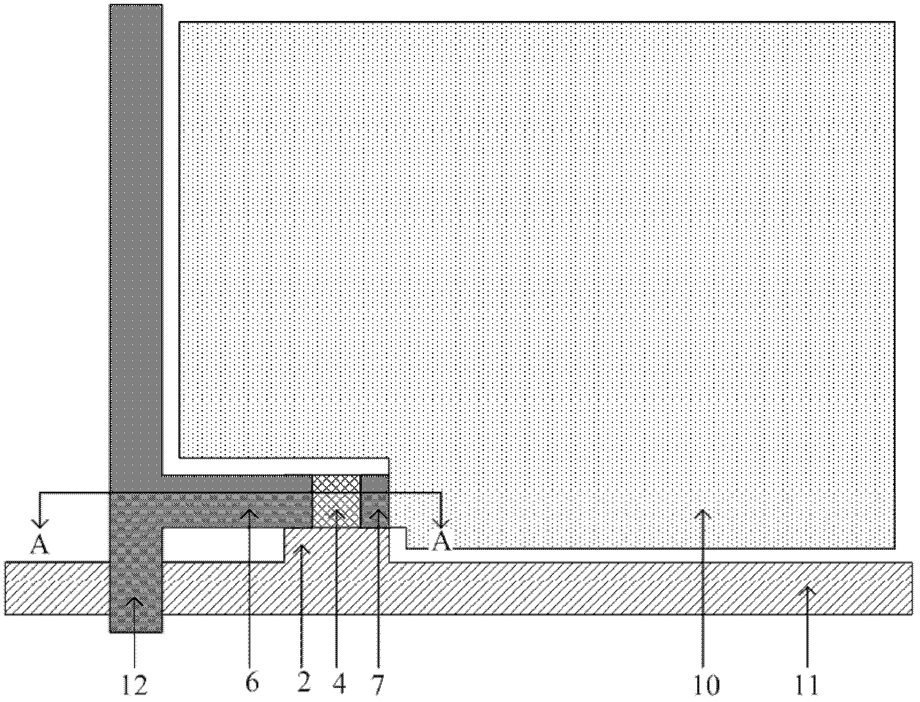
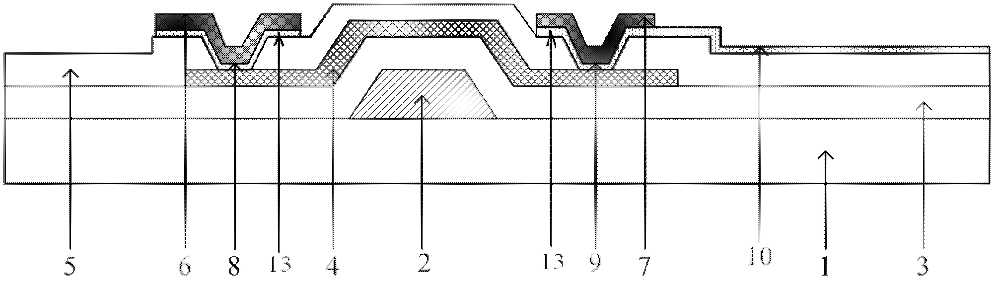
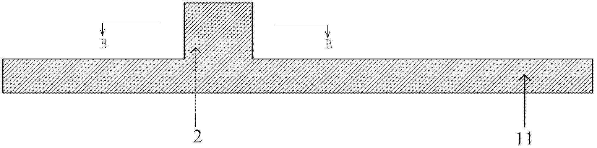
[0038] Such as figure 1 and figure 2 As shown, the liquid crystal display array substrate of the present invention includes: a substrate 1, gate scanning lines 11 and data lines 12 formed on the substrate 1, and a matrix arrangement formed by crossing the gate scanning lines 11 and data lines 12. Each pixel area includes at least one thin film transistor device and a pixel electrode 10; the thin film transistor device includes: gate electrode 2, metal oxide semiconductor layer 4, protective layer 5, source electrode 6 and drain electrode 7. Wherein, a gate insulating layer 3 is provided between the gate electrode 2 and the metal oxide semiconductor layer 4, a protective layer 5 is provided on the metal oxide semiconductor layer 4, and two There are three vias, which are the source electrode contact via hole 8 and the drain electrode contact via hole 9 respectively. ...


PUM

PropertyMeasurementUnit
sizeaaaaaaaaaa

Abstract

The invention discloses a liquid crystal display array substrate and a manufacturing method thereof as well as a liquid crystal display which are designed mainly aiming at the defects that an existing array substrate manufacturing process is complicated and low in production efficiency. The array substrate comprises a substrate, a gate electrode scanning line and a data line which are formed on the substrate, and pixel areas which are formed by the intersection of the grid electrode scanning line and the data line and arranged in a matrix form, wherein each pixel area at least comprises a thin film transistor device and a pixel electrode, the thin film transistor device comprises a gate electrode, a metal oxide semiconductor layer, a protective layer, a source electrode and a drain electrode, a gate insulation layer is arranged between the gate electrode and the metal oxide semiconductor layer, the metal oxide semiconductor layer is provided with the protective layer, and the source electrode and the drain electrode are respectively connected with the metal oxide semiconductor layer by virtue of through holes arranged on the protective layer. The array substrate is simple in manufacturing process and high in production efficiency, and can be used for avoiding the damage to the metal oxide semiconductor layer when the source electrode and the drain electrode are formed.

Description

technical field [0001] The invention relates to a liquid crystal display technology, in particular to a liquid crystal display array substrate, a manufacturing method thereof, and a liquid crystal display. Background technique [0002] In recent years, with the increasing size of liquid crystal displays and the increasing frequency of driving circuits, it is difficult for the mobility of existing amorphous silicon thin film transistors to meet the demand. The mobility of amorphous silicon thin film transistors is generally 0.5cm 2 / VS or so, the size of the liquid crystal display is more than 80 inches, and when the driving frequency is 120Hz, it needs 1cm 2 Mobility above / VS, it is obvious that the mobility of amorphous silicon is difficult to meet the demand. At present, metal oxide thin film transistors, such as amorphous IGZO, are popular for their high mobility, good uniformity, transparency, simple manufacturing process, and can meet the needs of large-size liquid c...

Claims


Application Information

Patent Timeline
Patent Type & Authority Applications(China)
IPC IPC(8): G02F1/1362G02F1/1368G03F7/00H01L29/786H01L21/77
Inventor 刘翔薛建设
Owner BOE TECH GRP CO LTD
Why Eureka
Try Eureka