Semiconductor light emitting diode (LED) device and formation method thereof

A technology of light-emitting diodes and semiconductors, applied in semiconductor devices, electrical components, circuits, etc., can solve the problems of high consumption of gold materials, high gold prices, and high electromigration, and achieve improved service life, improved thermal stability, and improved resistance to The effect of electromigration

Active Publication Date: 2012-09-12
HANGZHOU SILAN AZURE
View PDF6 Cites 9 Cited by
  • Summary
  • Abstract
  • Description
  • Claims
  • Application Information

AI Technical Summary

Problems solved by technology

However, aluminum has a low melting point (660°C) and high electromigration, which is not suitable for use as electrode materials for high-current and high-power chips. Gold is expensive, and gold layer electrodes generally have to be more than 1um. Evaporating quite thick gold will Lead to greater consumption of gold materials

Method used


Image

  • Semiconductor light emitting diode (LED) device and formation method thereof
  • Semiconductor light emitting diode (LED) device and formation method thereof
  • Semiconductor light emitting diode (LED) device and formation method thereof

Examples


no. 1 example

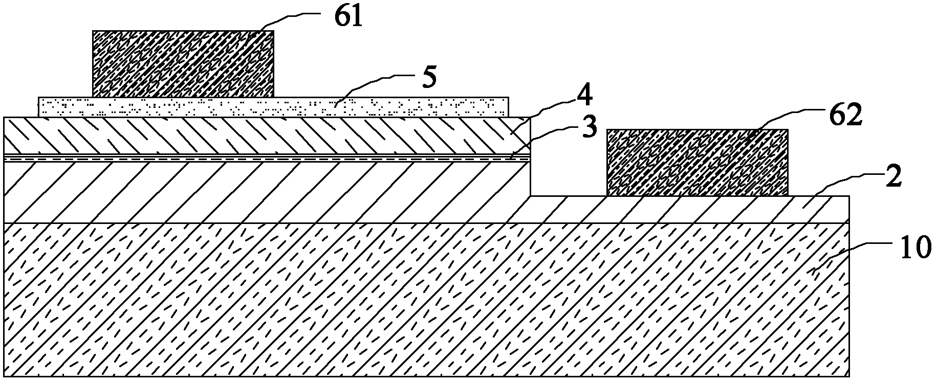
[0082] figure 1 The cross-sectional structure of the semiconductor light emitting diode device of the first embodiment is shown, including: a substrate 10; an N-type semiconductor layer 2, an active layer 3 and a P-type semiconductor layer 4 located on the substrate 10 in sequence; The extended electrode layer 5 on the top; the positive electrode welding layer 61 on the extended electrode layer 5; the trenches located in the P-type semiconductor layer 4, the active layer 3 and the N-type semiconductor layer 2, and the bottom of the trench exposes the N type semiconductor layer 2; the negative electrode welding layer 62 at the bottom of the trench. In this embodiment, the positive electrode welding layer 61 and the negative electrode welding layer 62 are located on the same side of the entire semiconductor light emitting diode device.

[0083] Wherein, the substrate 10 can be a sapphire substrate, the N-type semiconductor layer 2 can be an N-type doped III-V compound semicondu...

no. 2 example

[0095] The structure and forming method of the semiconductor light emitting diode device of the second embodiment are the same as those of the first embodiment, except that the thickness of the positive electrode welding layer 61 and the negative electrode welding layer 62 is 4 μm, and the material is an aluminum alloy of Al-1wt% Cu , the planar area of ​​the active layer 3 is 2025 square milliinches, and the forward voltage is 3.3V when working at 350mA.

no. 3 example

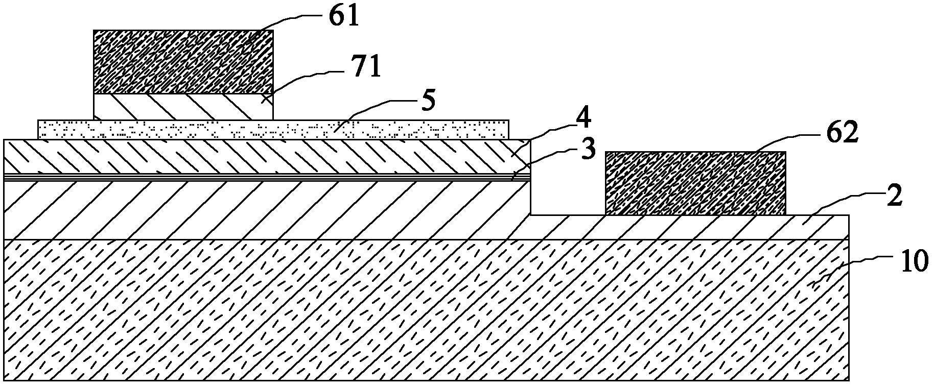
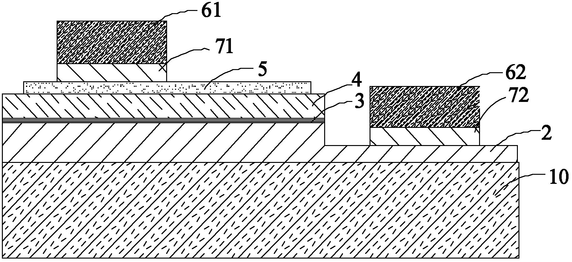
[0097] figure 2 The cross-sectional structure of the semiconductor light emitting diode device of the third embodiment is shown, and its structure and formation method are basically similar to those of the device in the first embodiment, except that a positive electrode contact layer 71 is formed on the extended electrode layer 5, and the positive electrode contact layer 71 is formed on the positive electrode layer 5. The electrode welding layer 61 is formed on the positive electrode contact layer 71 capable of reducing ohmic contact. In addition, a positive electrode transition layer (not shown in the figure) can also be formed between the positive electrode contact layer 71 and the positive electrode welding layer 61, and the positive electrode transition layer can be used to prevent the positive electrode welding layer 61 from contacting the extended electrode layer 5. Interdiffusion reaction, optional materials can be Ti, Pt, Ni, W, TiW, etc.

[0098]In the third embodim...


PUM


Abstract

The invention provides a semiconductor light emitting diode (LED) device and a formation method thereof. The semiconductor LED device comprises an active layer, a P-type semiconductor layer, an N-type semiconductor layer, a positive electrode welding layer and a negative electrode welding layer, wherein the P-type semiconductor layer and the N-type semiconductor layer are respectively positioned on two sides of the active layer; the positive electrode welding layer is electrically connected with the P-type semiconductor layer; the negative electrode welding layer is electrically connected with the N-type semiconductor layer; and the positive electrode welding layer and/or the negative electrode welding layer are/is made of an aluminum alloy material. Requirements of the LED device for the electrode welding layers can be well met, electro-migration resistance under large current can be improved, and the thermal stability of the device is improved. Compared with the conventional aluminum material, the aluminum alloy material has the advantages that the service life of the device is prolonged, and control over industrialization cost is facilitated.

Description

technical field [0001] The invention relates to a semiconductor light emitting diode device and a forming method thereof. Background technique [0002] In recent years, III-V compound semiconductor light-emitting diodes (LEDs) have attracted much attention. With the continuous marketization of LED products, the prices of chips and lamps are also dropping by an average of 20-30%. The key technologies of III-V compound semiconductor light-emitting diodes mainly include the growth of epitaxial wafers and the fabrication of electrodes on chips. [0003] In order to further reduce the manufacturing cost of LEDs, the industry is currently trying to use silicon and metal materials as substrate materials to develop high-power LEDs. However, with the continuous decline in the manufacturing cost of sapphire substrates, the cost advantages of silicon and metal materials are no longer obvious. However, silicon and other substrate materials still need to transfer the substrate in the l...

Claims


Application Information

Patent Timeline
Patent Type & Authority Applications(China)
IPC IPC(8): H01L33/40
CPCH01L33/32H01L33/40H01L2933/0016H01L33/0066H01L33/0075H01L33/0093
Inventor 张昊翔金豫浙封飞飞万远涛高耀辉李东昇江忠永
Owner HANGZHOU SILAN AZURE
Why Eureka
Try Eureka