
TFT substrate inspection apparatus and tft substrate inspection method

A substrate inspection and substrate technology, applied in identification devices, measuring devices, instruments, etc., can solve the problems of longer detection time and longer TFT substrate time, and achieve the effect of improving detection accuracy and shortening defect detection time

Inactive Publication Date: 2012-09-12
SHIMADZU SEISAKUSHO CO LTD
View PDF11 Cites 9 Cited by
  • Summary
  • Abstract
  • Description
  • Claims
  • Application Information

AI Technical Summary

Problems solved by technology

In this way, if the defect detection time becomes longer, the time required for the manufacturing steps of the TFT substrate will also be longer

Method used


Image

  • TFT substrate inspection apparatus and tft substrate inspection method
  • TFT substrate inspection apparatus and tft substrate inspection method
  • TFT substrate inspection apparatus and tft substrate inspection method

Examples


Embodiment Construction

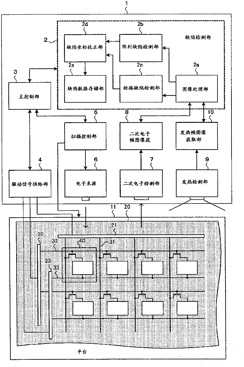
[0113] Hereinafter, embodiments of the present invention will be described in detail with reference to the drawings. figure 1 It is a schematic diagram of the TFT substrate inspection apparatus of the present invention.

[0114] The TFT substrate inspection apparatus 1 detects array defects and short-circuit defects of a TFT substrate 20 mounted on a stage 11 installed in a vacuum chamber (not shown).

[0115] The composition for detecting array defects includes: an electron beam source 6, which irradiates electron beams onto the TFT substrate 20; a platform 11, which moves the TFT substrate 20 along the x and y directions; a scanning control part 5, which controls the electron beam source 6 and The platform 11 controls the electron beam to scan on the TFT substrate 20; the secondary electron detection part 7 detects the secondary electrons released from the TFT substrate 20; the secondary electron frame image acquisition part 8 detects the secondary electrons according to th...


PUM


Abstract

Disclosed is a TFT substrate inspection apparatus which is provided with a defect detecting unit, which detects a defect of a TFT substrate, on the basis of detection signals outputted from a secondary electron detector and detection signals outputted from a heat detector. The defect detecting unit is provided with: a TFT array defect detecting unit, which detects a defect of a TFT array on the basis of the detection signals outputted from the secondary electron detector; and a short-circuit defect detecting unit, which detects a short-circuit defect on the basis of the detection signals outputted from a heat detector. The TFT array defect detecting unit detects a TFT array defect by sequentially selecting each of a plurality of panels provided on the substrate, and the short-circuit defect detecting unit performs short-circuit defect detection at one time for all the panels provided on the substrate. At the time of detecting a defect by means of electron beam irradiation and a short-circuit defect by means of heat detection with respect to the substrate having the panels formed thereon, a defect detection time necessary for the whole substrate is shortened.

Description

technical field [0001] The present invention relates to a thin film transistor (Thin Film Transistor, TFT) substrate inspection device used for TFT substrate inspection in the manufacturing steps of TFT panels (panels) such as liquid crystal substrates. In particular, the present invention relates to a TFT substrate inspection device suitable for short defect inspection. Background technique [0002] For the manufacturing process of a semiconductor substrate formed with a TFT array (array) such as a liquid crystal substrate or an organic electroluminescence (Electroluminescence, EL) substrate, a TFT array inspection step is included in the manufacturing process, and in the TFT array inspection step, the TFT arrays are inspected for defects. [0003] The TFT array is used, for example, as a switching element for selecting pixels (pixel electrodes) of a liquid crystal display device. On a substrate including a TFT array, for example, a plurality of gate lines functioning as ...

Claims


Application Information

Patent Timeline
Patent Type & Authority Applications(China)
IPC IPC(8): G01R31/00G01N23/225G02F1/13G02F1/1368G09F9/00G09F9/30
CPCG09G3/36G09G3/006
Inventor 今井大辅
Owner SHIMADZU SEISAKUSHO CO LTD
Learn More