Scanning data correcting device and drawing device

A data correction and data technology, which is applied in the direction of exposure devices, optics, and instruments in the photoengraving process.

Active Publication Date: 2014-08-13
DAINIPPON SCREEN MTG CO LTD
View PDF11 Cites 0 Cited by
  • Summary
  • Abstract
  • Description
  • Claims
  • Application Information

AI Technical Summary

Problems solved by technology

[0005] In the techniques described in Documents 1 and 2, since the drawing data is only corrected based on the position change of the alignment mark, and the end use method of the substrate to be manufactured, which is the object to be drawn, is not considered, it may occur in the post-process. Defective or yield deterioration
For example, in the case of using the build-up method of printed circuit boards, if the data for each drawing is corrected for the strain generated by deformation factors such as etching and pressing, the accumulation of the corrections will cause Potential for the resulting pattern to not match the size of the part mounted on it

Method used


Image

  • Scanning data correcting device and drawing device
  • Scanning data correcting device and drawing device
  • Scanning data correcting device and drawing device

Examples


Embodiment Construction

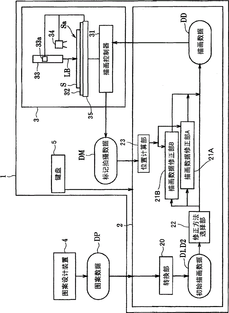
[0035] The structure of the drawing device

[0036] figure 1 It is a figure which shows the schematic structure of the drawing apparatus 1 which concerns on embodiment of this invention. The drawing device 1 is a direct drawing device (direct drawing device) that irradiates a laser light LB as exposure light and scans with the laser light LB to draw a part of a substrate S that is a drawing target such as a printed substrate, a semiconductor substrate, a liquid crystal substrate, etc. By performing exposure continuously, the exposure image of a desired circuit pattern is drawn on the board|substrate S. As shown in FIG.

[0037] The drawing device 1 is mainly composed of the following structures: a data processing device 2 that generates drawing data DD and also corrects necessary data; an exposure device 3 that performs actual drawing based on the drawing data DD (Exposure); a keyboard 5 serving as an information input unit for inputting information to the data processing de...


PUM


Abstract

A scanning data correcting device and a drawing device are provided. In the scanning data correcting device, a correction method selection part selectively uses a plurality of data correction parts according to received correction information, so as to correct drawing data. The drawing device draws a substrate based on the corrected drawing data (DD). Thus a correction method is selected according to the substrate to be manufactured. Therefore, the drawing data can be corrected in a way suitable for subsequent processes or application.

Description

technical field [0001] The present invention relates to a drawing data correction device and a drawing device, and more particularly to a drawing data correction device and a drawing device related to the manufacture of substrates such as printed boards, semiconductor substrates, and liquid crystal substrates. Background technique [0002] Heretofore, there has been known a direct drawing device (direct drawing device) that continuously draws an object (hereinafter, also simply referred to as a substrate) on a printed substrate, a semiconductor substrate, a liquid crystal substrate, etc., by scanning and irradiating exposure light such as a laser. ) is a device that exposes a part of the circuit and draws a desired circuit pattern to form a circuit pattern. [0003] The direct drawing device draws the circuit diagram based on drawing data converted based on the design data of the circuit diagram and having a description format that the direct drawing device can handle. Amon...

Claims


Application Information

Patent Timeline
Patent Type & Authority Patents(China)
IPC IPC(8): G03F7/20G03F9/00
CPCG03F1/36G03F1/72G03F7/70491G03F7/70508G03F7/70791H01J37/3174
Inventor 八坂智山田亮
Owner DAINIPPON SCREEN MTG CO LTD
Why Eureka
Try Eureka